- 您现在的位置:买卖IC网 > PDF目录9481 > LTC1093CSW#PBF (Linear Technology)IC DATA ACQ SYS 10BIT 6CH 16SOIC PDF资料下载
参数资料
| 型号: | LTC1093CSW#PBF |
| 厂商: | Linear Technology |
| 文件页数: | 27/32页 |
| 文件大小: | 0K |
| 描述: | IC DATA ACQ SYS 10BIT 6CH 16SOIC |
| 标准包装: | 47 |
| 类型: | 数据采集系统(DAS),ADC |
| 分辨率(位): | 10 b |
| 数据接口: | 串行 |
| 电压电源: | 双 ± |
| 电源电压: | ±5V,4.5V,10V |
| 工作温度: | -40°C ~ 85°C |
| 安装类型: | 表面贴装 |
| 封装/外壳: | 16-SOIC(0.295",7.50mm 宽) |
| 供应商设备封装: | 16-SOIC |
| 包装: | 管件 |
第1页第2页第3页第4页第5页第6页第7页第8页第9页第10页第11页第12页第13页第14页第15页第16页第17页第18页第19页第20页第21页第22页第23页第24页第25页第26页当前第27页第28页第29页第30页第31页第32页
4
LTC1091/LTC1092
LTC1093/LTC1094
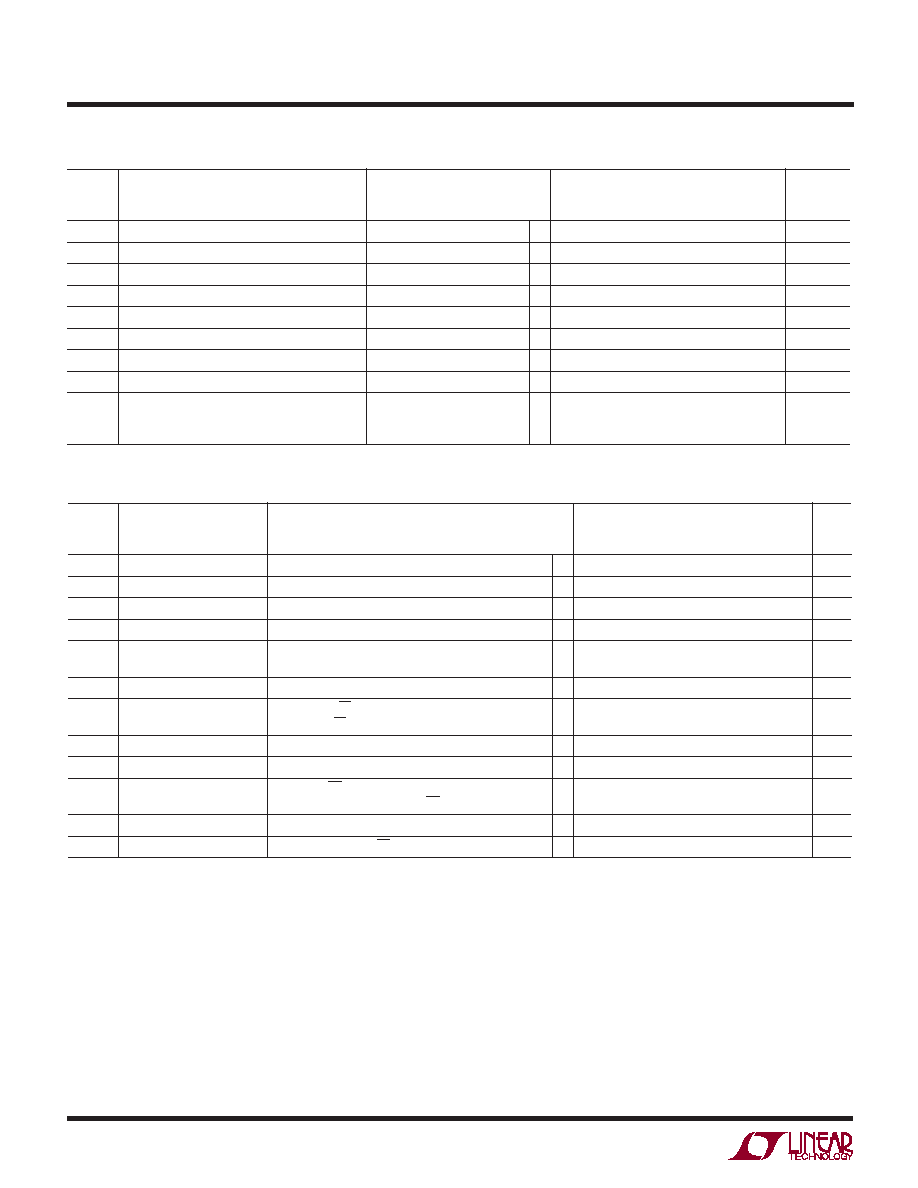
AC CHARACTERISTICS
The q denotes specifications which apply over the full operating temperature range, otherwise specifications are TA = 25°C. (Note 3)
LTC1091A/LTC1092A/LTC1093A/LTC1094A
LTC1091/LTC1092/LTC1093/LTC1094
SYMBOL
PARAMETER
CONDITIONS
MIN
TYP
MAX
UNITS
tSMPL
Analog Input Sample Time
See Operating Sequence
1.5
CLK Cycles
tCONV
Conversion Time
See Operating Sequence
10
CLK Cycles
tdDO
Delay Time, CLK
↓ to DOUT Data Valid
See Test Circuits
q
400
850
ns
tdis
Delay Time, CS
↑ to DOUT Hi-Z
See Test Circuits
q
180
450
ns
ten
Delay Time, CLK
↓ to DOUT Enabled
See Test Circuits
q
160
450
ns
thDO
Time Output Data Remains Valid After SCLK
↓
150
ns
tf
DOUT Fall Time
See Test Circuits
q
90
300
ns
tr
DOUT Rise Time
See Test Circuits
q
60
300
ns
CIN
Input Capacitance
Analog Inputs On-Channel
65
pF
Analog Inputs Off-Channel
5
pF
Digital Inputs
5
pF
The q denotes specifications which apply over the full operating temperature range, otherwise specifications are TA = 25°C. (Note 3)
ELECTRICAL C
C
HARA TER STICS
DIGITAL A D
U
I
DC
LTC1091A/LTC1092A/LTC1093A/LTC1094A
LTC1091/LTC1092/LTC1093/LTC1094
SYMBOL PARAMETER
CONDITIONS
MIN
TYP
MAX
UNITS
VIH
High Level Input Voltage
VCC = 5.25V
q
2.0
V
VIL
Low Level Input Voltage
VCC = 4.75V
q
0.8
V
IIH
High Level Input Current
VIN = VCC
q
2.5
A
IIL
Low Level Input Current
VIN = 0V
q
–2.5
A
VOH
High Level Output Voltage
VCC = 4.75V, IOUT = 10
A
4.7
V
VCC = 4.75V, IOUT = 360
A
q
2.4
4.0
V
VOL
Low Level Output Voltage
VCC = 4.75V, IOUT = 1.6mA
q
0.4
V
IOZ
Hi-Z Output Leakage
VOUT = VCC, CS High
q
3
A
VOUT = 0V, CS High
q
–3
A
ISOURCE
Output Source Current
VOUT = 0V
–10
mA
ISINK
Output Sink Current
VOUT = VCC
10
mA
ICC
Positive Supply Current
LTC1091, CS High
q
1.5
3.5
mA
LTC1092/LTC1093/LTC1094, CS High, REF + Open
q
1.0
2.5
mA
IREF
Reference Current
LTC1092/LTC1093/LTC1094, VREF = 5V
q
0.5
1.0
mA
I –
Negative Supply Current
LTC1093/LTC1094, CS High, V – = – 5V
q
150
A
Note 1: Absolute Maximum Ratings are those values beyond which the life
of a device may be impaired.
Note 2: All voltage values are with respect to ground with DGND, AGND,
GND and REF
– wired together (unless otherwise noted). REF– is internally
connected to the AGND pin on the LTC1093. DGND, AGND, REF– and V–
are internally connected to the GND pin on the LTC1091/LTC1092.
Note 3: VCC = 5V, VREF
+ = 5V, VREF– = 0V, V– = 0V for unipolar mode and
– 5V for bipolar mode, CLK = 0.5MHz unless otherwise specified.
Note 4: These specs apply for both unipolar (LTC1091/LTC1092/LTC1093/
LTC1094) and bipolar (LTC1093/LTC1094 only) modes. In bipolar mode,
one LSB is equal to the bipolar input span (2VREF) divided by 1024. For
example, when VREF = 5V, 1LSB (bipolar) = 2(5V)/1024 = 9.77mV.
Note 5: Linearity error is specified between the actual end points of the
A/D transfer curve.
Note 6: Total unadjusted error includes offset, full scale, linearity,
multiplexer and hold step errors.
Note 7: Two on-chip diodes are tied to each reference and analog input
which will conduct for reference or analog input voltages one diode drop
below V – or one diode drop above VCC. Be careful during testing at low
VCC levels (4.5V), as high level reference or analog inputs (5V) can cause
this input diode to conduct, especially at elevated temperatures, and cause
errors for inputs near full scale. This spec allows 50mV forward bias of
either diode. This means that as long as the reference or analog input does
not exceed the supply voltage by more than 50mV, the output code will be
correct. To achieve an absolute 0V to 5V input voltage range will therefore
require a minimum supply voltage of 4.950V over initial tolerance,
temperature variations and loading.
Note 8: Channel leakage current is measured after the channel selection.
相关PDF资料 |
PDF描述 |
|---|---|
| LTC1093CSW | IC DATA ACQ SYS 10BIT 6CH 16SOIC |
| V24A5M300BF3 | CONVERTER MOD DC/DC 5V 300W |
| V24A5M300B | CONVERTER MOD DC/DC 5V 300W |
| LTC1296BCN | IC DATA ACQ SYSTEM 12BIT 20-DIP |
| V24A3V3M200B | CONVERTER MOD DC/DC 3.3V 200W |
相关代理商/技术参数 |
参数描述 |
|---|---|
| LTC1093MJ | 制造商:Linear Technology 功能描述:Single ADC SAR 26ksps 10-bit Serial 16-Pin CDIP |
| LTC1094 | 制造商:LINER 制造商全称:Linear Technology 功能描述:1-, 2-, 6- and 8-Channel, 10-Bit Serial I/O Data Acquisition Systems |
| LTC1094AC | 制造商:LINER 制造商全称:Linear Technology 功能描述:1-, 2-, 6- and 8-Channel, 10-Bit Serial I/O Data Acquisition Systems |
| LTC1094ACN | 功能描述:IC DATA ACQ SYS 10BIT 8CH 20-DIP RoHS:否 类别:集成电路 (IC) >> 数据采集 - ADCs/DAC - 专用型 系列:- 产品培训模块:Lead (SnPb) Finish for COTS Obsolescence Mitigation Program 标准包装:50 系列:- 类型:数据采集系统(DAS) 分辨率(位):16 b 采样率(每秒):21.94k 数据接口:MICROWIRE?,QSPI?,串行,SPI? 电压电源:模拟和数字 电源电压:1.8 V ~ 3.6 V 工作温度:-40°C ~ 85°C 安装类型:表面贴装 封装/外壳:40-WFQFN 裸露焊盘 供应商设备封装:40-TQFN-EP(6x6) 包装:托盘 |
| LTC1094ACN#PBF | 功能描述:IC DATA ACQ SYS 10BIT 8CH 20-DIP RoHS:是 类别:集成电路 (IC) >> 数据采集 - ADCs/DAC - 专用型 系列:- 产品培训模块:Lead (SnPb) Finish for COTS Obsolescence Mitigation Program 标准包装:50 系列:- 类型:数据采集系统(DAS) 分辨率(位):16 b 采样率(每秒):21.94k 数据接口:MICROWIRE?,QSPI?,串行,SPI? 电压电源:模拟和数字 电源电压:1.8 V ~ 3.6 V 工作温度:-40°C ~ 85°C 安装类型:表面贴装 封装/外壳:40-WFQFN 裸露焊盘 供应商设备封装:40-TQFN-EP(6x6) 包装:托盘 |
发布紧急采购,3分钟左右您将得到回复。