- 您现在的位置:买卖IC网 > PDF目录10333 > LTC1096ACS8#PBF (Linear Technology)IC A/D CONV 8BIT SRL IN/OUT8SOIC PDF资料下载
参数资料
| 型号: | LTC1096ACS8#PBF |
| 厂商: | Linear Technology |
| 文件页数: | 31/32页 |
| 文件大小: | 0K |
| 描述: | IC A/D CONV 8BIT SRL IN/OUT8SOIC |
| 标准包装: | 100 |
| 位数: | 8 |
| 采样率(每秒): | 33k |
| 数据接口: | 串行 |
| 转换器数目: | 1 |
| 功率耗散(最大): | 600µW |
| 电压电源: | 单电源 |
| 工作温度: | 0°C ~ 70°C |
| 安装类型: | 表面贴装 |
| 封装/外壳: | 8-SOIC(0.154",3.90mm 宽) |
| 供应商设备封装: | 8-SOIC |
| 包装: | 管件 |
| 输入数目和类型: | 1 个差分,单极 |
第1页第2页第3页第4页第5页第6页第7页第8页第9页第10页第11页第12页第13页第14页第15页第16页第17页第18页第19页第20页第21页第22页第23页第24页第25页第26页第27页第28页第29页第30页当前第31页第32页
LTC1096/LTC1096L
LTC1098/LTC1098L
8
10968fc
Note 1: Stresses beyond those listed under Absolute Maximum Ratings
may cause permanent damage to the device. Exposure to any Absolute
Maximum Rating condition for extended periods may affect device
reliability and lifetime.
Note 2: All voltage values are with respect to GND.
Note 3: For the 8-lead PDIP, consult the factory.
Note 4: Linearity error is specied between the actual and points of the
A/D transfer curve.
Note 5: Total unadjusted error includes offset, full scale, linearity,
multiplexer and hold step errors.
Note 6: Two on-chip diodes are tied to each reference and analog input
which will conduct for reference or analog input voltages one diode
drop below GND or one diode drop above VCC. This spec allows 50mV
forward bias of either diode. This means that as long as the reference or
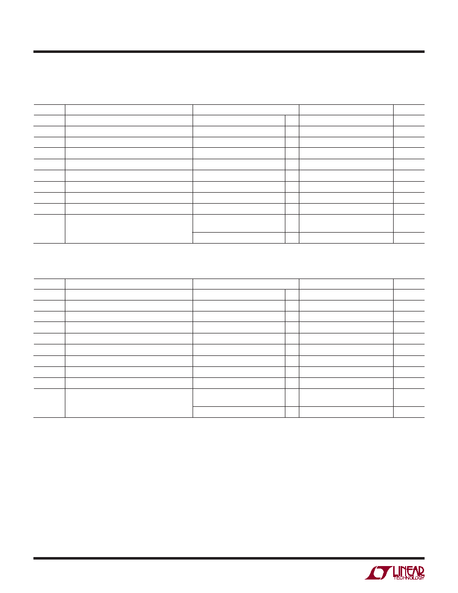
SYMBOL
PARAMETER
CONDITIONS
MIN
TYP
MAX
UNITS
tSMPL
Analog Input Sample Time
See Operating Sequence
1.5
CLK Cycles
fSMPL(MAX) Maximum Sampling Frequency
l
16.5
kHz
tCONV
Conversion Time
See Operating Sequence
8
CLK Cycles
tdDO
Delay Time, CLK
↓ to DOUT Data Valid
See Test Circuits (Note 9)
l
500
1000
ns
tdis
Delay Time, CS
↑ to DOUT Hi-Z
See Test Circuits (Note 9)
l
220
800
ns
ten
Delay Time, CLK
↓ to DOUT Enable
See Test Circuits (Note 9)
l
160
480
ns
thDO
Time Output Data Remains Valid After CLK
↓
CLOAD = 100pF
400
ns
tf
DOUT Fall Time
See Test Circuits (Note 9)
l
70
250
ns
tr
DOUT Rise Time
See Test Circuits (Note 9)
l
50
150
ns
CIN
Input Capacitance
Analog Inputs On Channel
Analog Inputs Off Channel
25
5
pF
Digital Input
5
pF
AC CHARACTERISTICS
LTC1096/LTC1098
The
l denotes the specications which apply over the full operating temperature range, otherwise specications are at TA = 25°C.
VCC = 3V, VREF = 2.5V, fCLK = 250kHz, unless otherwise noted.
SYMBOL
PARAMETER
CONDITIONS
MIN
TYP
MAX
UNITS
tSMPL
Analog Input Sample Time
See Operating Sequence
1.5
CLK Cycles
fSMPL(MAX) Maximum Sampling Frequency
l
16.5
kHz
tCONV
Conversion Time
See Operating Sequence
8
CLK Cycles
tdDO
Delay Time, CLK
↓ to DOUT Data Valid
See Test Circuits
l
500
1000
ns
tdis
Delay Time, CS
↑ to DOUT Hi-Z
See Test Circuits
l
220
800
ns
ten
Delay Time, CLK
↓ to DOUT Enable
See Test Circuits
l
160
480
ns
thDO
Time Output Data Remains Valid After CLK
↓
CLOAD = 100pF
400
ns
tf
DOUT Fall Time
See Test Circuits
l
70
250
ns
tr
DOUT Rise Time
See Test Circuits
l
50
200
ns
CIN
Input Capacitance
Analog Inputs On Channel
Analog Inputs Off Channel
25
5
pF
Digital Input
5
pF
LTC1096L/LTC1098L
The
l denotes the specications which apply over the full operating temperature range, otherwise specications are at TA = 25°C.
VCC = 2.65V, VREF = 2.5V, fCLK = 250kHz, unless otherwise noted.
analog input does not exceed the supply voltage by more than 50mV, the
output code will be correct. To achieve an absolute 0V to 5V input voltage
range will therefore require a minimum supply voltage of 4.950V over
initial tolerance, temperature variations and loading. For 5.5V < VCC ≤ 9V,
reference and analog input range cannot exceed 5.55V. If reference and
analog input range are greater than 5.55V, the output code will not be
guaranteed to be correct.
Note 7: The supply voltage range for the LTC1096L/LTC1098L is from
2.65V to 4V. The supply voltage range for the LTC1096 is from 3V to 9V,
but the supply voltage range for the LTC1098 is only from 3V to 6V.
Note 8: Channel leakage current is measured after the channel selection.
Note 9: These specications are either correlated from 5V specications or
guaranteed by design.
相关PDF资料 |
PDF描述 |
|---|---|
| D38999/20JF11PNLC | CONN HSG RCPT 11POS WALL MT PINS |
| D38999/24WA98BA | CONN HSG RCPT 3POS JAM NUT SCKT |
| LTC1096ACS8 | IC A/D CONV 8BIT SRL IN/OUT8SOIC |
| LTC1096ACN8#PBF | IC A/D CONV 8BIT SRL IN/OUT 8DIP |
| LTC1096ACN8 | IC A/D CONV 8BIT SRL IN/OUT 8DIP |
相关代理商/技术参数 |
参数描述 |
|---|---|
| LTC1096ACS8-TR | 制造商:LINER 制造商全称:Linear Technology 功能描述:Micropower Sampling 8-Bit Serial I/O A/D Converters |
| LTC1096ACS8-TRPBF | 制造商:LINER 制造商全称:Linear Technology 功能描述:Micropower Sampling 8-Bit Serial I/O A/D Converters |
| LTC1096AI | 制造商:LINER 制造商全称:Linear Technology 功能描述:Micropower Sampling 8-Bit Serial I/O A/D Converters |
| LTC1096AIN8 | 功能描述:IC ADC 8BIT SERIAL I/O 5V 8DIP RoHS:否 类别:集成电路 (IC) >> 数据采集 - 模数转换器 系列:- 标准包装:2,500 系列:- 位数:16 采样率(每秒):15 数据接口:MICROWIRE?,串行,SPI? 转换器数目:1 功率耗散(最大):480µW 电压电源:单电源 工作温度:-40°C ~ 85°C 安装类型:表面贴装 封装/外壳:38-WFQFN 裸露焊盘 供应商设备封装:38-QFN(5x7) 包装:带卷 (TR) 输入数目和类型:16 个单端,双极;8 个差分,双极 配用:DC1011A-C-ND - BOARD DELTA SIGMA ADC LTC2494 |
| LTC1096AIN8#PBF | 功能描述:IC ADC 8BIT SERIAL I/O 5V 8DIP RoHS:是 类别:集成电路 (IC) >> 数据采集 - 模数转换器 系列:- 标准包装:2,500 系列:- 位数:16 采样率(每秒):15 数据接口:MICROWIRE?,串行,SPI? 转换器数目:1 功率耗散(最大):480µW 电压电源:单电源 工作温度:-40°C ~ 85°C 安装类型:表面贴装 封装/外壳:38-WFQFN 裸露焊盘 供应商设备封装:38-QFN(5x7) 包装:带卷 (TR) 输入数目和类型:16 个单端,双极;8 个差分,双极 配用:DC1011A-C-ND - BOARD DELTA SIGMA ADC LTC2494 |
发布紧急采购,3分钟左右您将得到回复。