- 您现在的位置:买卖IC网 > PDF目录10235 > LTC1099CSW (Linear Technology)IC A/D CONV 8BIT HI-SPEED 20SOIC PDF资料下载
参数资料
| 型号: | LTC1099CSW |
| 厂商: | Linear Technology |
| 文件页数: | 16/16页 |
| 文件大小: | 0K |
| 描述: | IC A/D CONV 8BIT HI-SPEED 20SOIC |
| 标准包装: | 38 |
| 位数: | 8 |
| 采样率(每秒): | 400k |
| 数据接口: | 并联 |
| 转换器数目: | 3 |
| 功率耗散(最大): | 55mW |
| 电压电源: | 单电源 |
| 工作温度: | 0°C ~ 70°C |
| 安装类型: | 表面贴装 |
| 封装/外壳: | 20-SOIC(0.295",7.50mm 宽) |
| 供应商设备封装: | 20-SOIC |
| 包装: | 管件 |
| 输入数目和类型: | 1 个单端,单极 |
| 其它名称: | LTC1099CS |
LTC1099
9
When RD goes low, with CS low, the result of the previous
conversion is output. This data stays there until the
ongoing conversion is complete (INT goes low). At this
time the outputs are updated with new data.
As long as CS and RD stay low long enough, the receiving
device will get the right data. Remember, the receiving
device reads data in on the rising edge of RD. The RDY
output facilitates making RD long enough.
In the RD mode, the WR input becomes the RDY output.
On the falling edge of RD, the RDY goes low. It is an open
drain output to allow a wired OR function so it requires a
pull-up resistor. At the end of conversion, the active pull-
down is released and RDY goes high.
The RDY output is designed to interface to the Ready In
(RDYIN) function on many popular processors. RDYIN
allows these processors to work with slow memory by
stretching the RD strobe coming from the processor. RD
will remain low as long as RDY is low. In the case of the
LTC1099, RDY stays low until the conversion is complete
and new data is available on the outputs. This greatly
simplifies the programmers task. Each time data is re-
quired from the A/D a simple read is executed. The
hardware interface makes sure the RD strobe is long
enough.
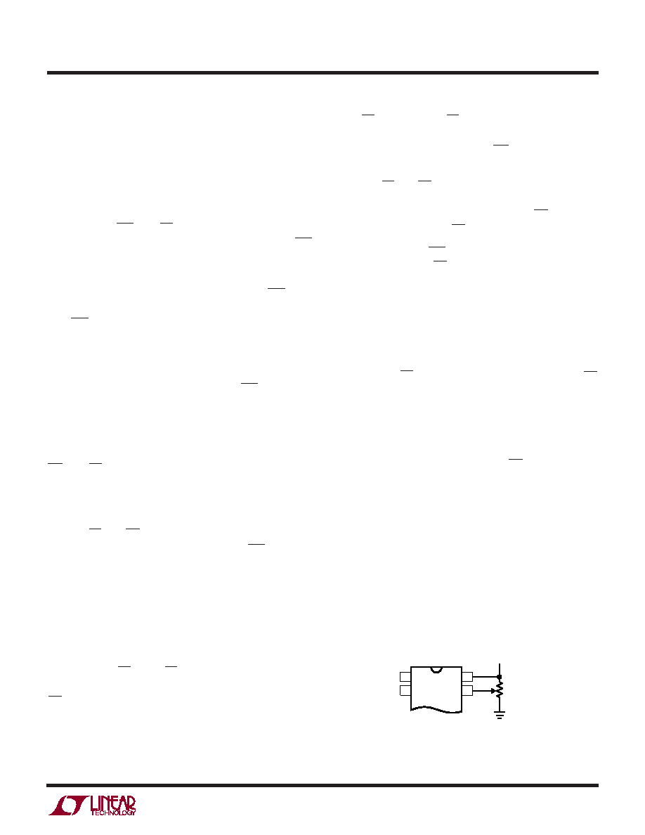
Adjusting the Conversion Time
The conversion time of the LTC1099 is internally set at
2.5
s. If desired, it can be adjusted by forcing a voltage on
Pin 19. With Pin 19 left open, the conversion time runs
2.5
s. A convenient way to force the voltage is with the
circuit shown in Figure 7. To preset the conversion time to
a fixed amount, a resistor may be tied from Pin 19 to VCC
or GND. Tying it to VCC slows down the conversion and
tying it to GND will speed it up (see Typical Performance
Characteristics).
DIGITAL I
U
TERFACE
The digital interface to the LTC1099 entails either control-
ling the conversion timing or reading data. There are two
basic modes for controlling and reading the A/D — the
Write-Read(WR-RD) mode and the Read (RD) mode.
WR-RD Mode (Pin 7 = High)
In the WR-RD mode, a conversion sequence starts on the
falling edge of WR with CS low (Figures 3a and 3b). This
is an edge-sensitive control function. The width of the WR
input is not important. All timing functions are internal to
the A/D.
The first thing to happen after the falling edge of WR is the
internal S/H is switched to hold. This typically takes 110ns
after WR falls and is the aperture time of the S/H.
Next, the A/D conversion takes place. The conversion time
is internally set at 2.5
s, but is user adjustable (see
Adjusting the Conversion Time). The end of conversion is
signaled by the high to low transition of INT. The S/H is
switched back to the acquire state as soon as the conver-
sion is complete.
After the conversion is complete, the 8-bit result is avail-
able on the three-state outputs. The outputs are active with
RD and CS low. Output data is latched and, if no new
conversion is initiated, is available indefinitely as long as
the power is not turned off.
The WR-RD mode is also used for stand-alone operation.
By tying CS and RD low the data outputs will be continu-
ously active (Figure 4). The falling edge of WR starts the
conversion sequence and when done new data will appear
on the outputs. All outputs will be updated simultaneously.
In stand-alone operation, the outputs will never be in a
high impedance state.
RD Mode (Pin 7 = Low)
In the RD mode, a conversion sequence is initiated by the
falling edge of RD when CS is low (Figure 2). The S/H is
switched to the hold state 110ns after the falling edge of
RD. It is switched back to the acquire state at the end of
conversion.
1
2
20
19
5V
10k
1099 F07
Figure 7. Adjusting the Conversion Time
相关PDF资料 |
PDF描述 |
|---|---|
| QGP323 | CONN PLUG CORD 3POS MALE |
| E4MSCBAU | CONN RCPT 4POS MALE SLD CUP GOLD |
| VI-21W-IU-F2 | CONVERTER MOD DC/DC 5.5V 200W |
| VI-J6W-MX-S | CONVERTER MOD DC/DC 5.5V 75W |
| VI-23K-CU-F1 | CONVERTER MOD DC/DC 40V 200W |
相关代理商/技术参数 |
参数描述 |
|---|---|
| LTC1099CSW#PBF | 功能描述:IC A/D CONV 8BIT HI-SPEED 20SOIC RoHS:是 类别:集成电路 (IC) >> 数据采集 - 模数转换器 系列:- 标准包装:1,000 系列:- 位数:12 采样率(每秒):300k 数据接口:并联 转换器数目:1 功率耗散(最大):75mW 电压电源:单电源 工作温度:0°C ~ 70°C 安装类型:表面贴装 封装/外壳:24-SOIC(0.295",7.50mm 宽) 供应商设备封装:24-SOIC 包装:带卷 (TR) 输入数目和类型:1 个单端,单极;1 个单端,双极 |
| LTC1099CSW#TR | 功能描述:IC ADC 8BIT SAMPL/HOLD HS 20SOIC RoHS:否 类别:集成电路 (IC) >> 数据采集 - 模数转换器 系列:- 标准包装:1,000 系列:- 位数:12 采样率(每秒):300k 数据接口:并联 转换器数目:1 功率耗散(最大):75mW 电压电源:单电源 工作温度:0°C ~ 70°C 安装类型:表面贴装 封装/外壳:24-SOIC(0.295",7.50mm 宽) 供应商设备封装:24-SOIC 包装:带卷 (TR) 输入数目和类型:1 个单端,单极;1 个单端,双极 |
| LTC1099CSW#TRPBF | 功能描述:IC A/D CONV 8BIT HI-SPEED 20SOIC RoHS:是 类别:集成电路 (IC) >> 数据采集 - 模数转换器 系列:- 标准包装:1,000 系列:- 位数:12 采样率(每秒):300k 数据接口:并联 转换器数目:1 功率耗散(最大):75mW 电压电源:单电源 工作温度:0°C ~ 70°C 安装类型:表面贴装 封装/外壳:24-SOIC(0.295",7.50mm 宽) 供应商设备封装:24-SOIC 包装:带卷 (TR) 输入数目和类型:1 个单端,单极;1 个单端,双极 |
| LTC1099I | 制造商:LINER 制造商全称:Linear Technology 功能描述:High Speed 8-Bit A/D Converter with Built-In Sample-and-Hold |
| LTC1099IJ | 制造商:LINER 制造商全称:Linear Technology 功能描述:High Speed 8-Bit A/D Converter with Built-In Sample-and-Hold |
发布紧急采购,3分钟左右您将得到回复。