- 您现在的位置:买卖IC网 > PDF目录14081 > LTC1144IS8 (Linear Technology)IC REG SWITCHED CAP INV 8SOIC PDF资料下载
参数资料
| 型号: | LTC1144IS8 |
| 厂商: | Linear Technology |
| 文件页数: | 6/8页 |
| 文件大小: | 0K |
| 描述: | IC REG SWITCHED CAP INV 8SOIC |
| 标准包装: | 100 |
| 类型: | 切换式电容器(充电泵),反相 |
| 输出数: | 1 |
| 输入电压: | 2 V ~ 18 V |
| 频率 - 开关: | 4kHz ~ 10kHz |
| 电流 - 输出: | 50mA |
| 同步整流器: | 无 |
| 工作温度: | -40°C ~ 85°C |
| 安装类型: | 表面贴装 |
| 封装/外壳: | 8-SOIC(0.154",3.90mm 宽) |
| 包装: | 管件 |
| 供应商设备封装: | 8-SOIC |
�� �
�
�LTC1144�
�A� PPLICATI�
�S� I� FOR� ATIO�
�and� hence� the� efficiency,� is� set� by� the� output� impedance.�
�As� frequency� is� decreased,� the� output� impedance� will�
�V� +�
�eventually� be� dominated� by� the� 1/(f� � C1)� term� and� power�
�efficiency� will� drop.�
�BOOST�
�9I�
�I�
�(1)�
�Note� also� that� power� efficiency� decreases� as� frequency�
�goes� up.� This� is� caused� by� internal� switching� losses� which�
�occur� due� to� some� finite� charge� being� lost� on� each�
�switching� cycle.� This� charge� loss� per� unit� cycle,� when�
�OSC�
�(7)�
�SCHMITT�
�TRIGGER�
�multiplied� by� the� switching� frequency,� becomes� a� current�
�loss.� At� high� frequency� this� loss� becomes� significant� and�
�the� power� efficiency� starts� to� decrease.�
�GND�
�(3)�
�9I�
�I�
�1144� F06�
�≈� 20pF�
�100�
�95�
�V� +� =� 15V,� C1� =� C2� =� 10� μ� F�
�I� L� =� 20mA,� T� A� =� 25°C�
�600�
�500�
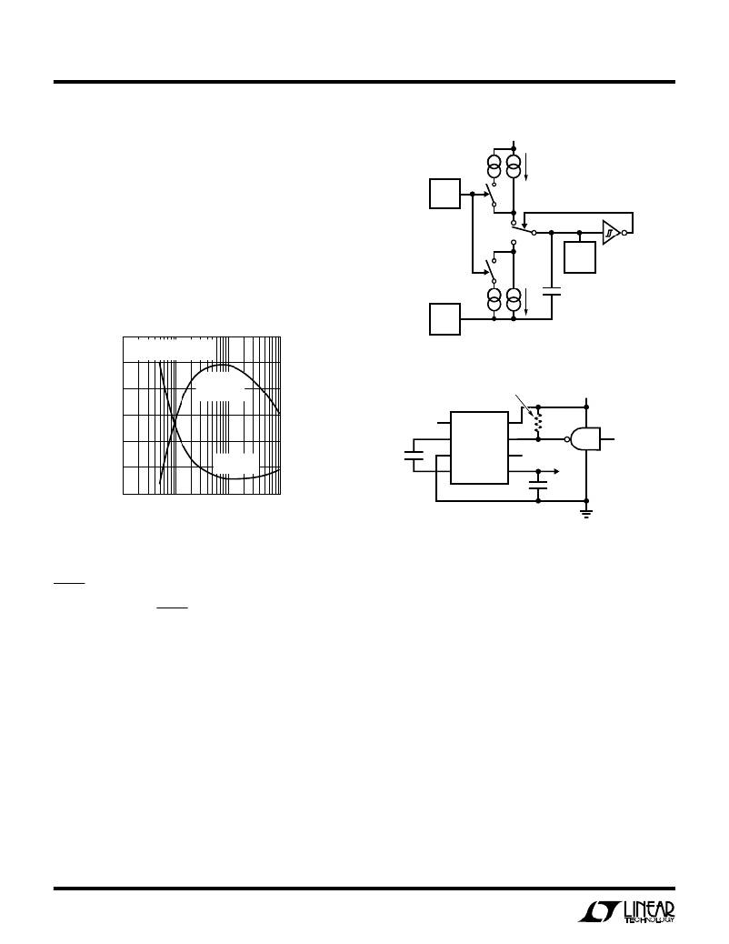
�Figure� 6.� Oscillator�
�POWER�
�90�
�CONVERSION�
�EFFICIENCY�
�400�
�REQUIRED� FOR�
�TTL� LOGIC�
�V� +�
�85�
�300�
�NC�
�1�
�8�
�100k�
�80�
�75�
�OUTPUT�
�RESISTANCE�
�200�
�100�
�C1�
�+�
�2�
�3�
�4�
�LTC1144�
�7�
�6�
�5�
�–(V� +� )�
�OSC� INPUT�
�C2�
�70�
�0.1�
�1� 10�
�0�
�100�
�1144� F07�
�OSCILLATOR� FREQUENCY� (kHz)�
�1144� F05�
�Figure� 7.� External� Clocking�
�Figure� 5.� Power� Conversion� Efficiency� and� Output�
�Resistance� vs� Oscillator� Frequency�
�SHDN� (Pin� 6)�
�The� LTC1144� has� a� SHDN� pin� that� will� disable� the� internal�
�oscillator� when� it� is� pulled� low.� The� supply� current� will� also�
�drop� to� 8� μ� A.�
�OSC� (Pin� 7)� and� Boost� (Pin� 1)�
�The� switching� frequency� can� be� raised,� lowered� or� driven�
�from� an� external� source.� Figure� 6� shows� a� functional�
�diagram� of� the� oscillator� circuit.�
�By� connecting� the� boost� pin� (pin� 1)� to� V� +� ,� the� charge� and�
�discharge� current� is� increased,� and� hence� the� frequency� is�
�increased� by� approximately� 10� times.� Increasing� the� fre-�
�quency� will� decrease� output� impedance� and� ripple� for�
�higher� load� currents.�
�Loading� pin� 7� with� more� capacitance� will� lower� the� fre-�
�quency.� Using� the� boost� (pin� 1)� in� conjunction� with� exter-�
�6�
�nal� capacitance� on� pin� 7� allows� user� selection� of� the�
�frequency� over� a� wide� range.�
�Driving� the� LTC1144� from� an� external� frequency� source�
�can� be� easily� achieved� by� driving� pin� 7� and� leaving� the�
�boost� pin� open� as� shown� in� Figure� 7.� The� output� current�
�from� pin� 7� is� small,� typically� 4� μ� A,� so� a� logic� gate� is� capable�
�of� driving� this� current.� The� choice� of� using� a� CMOS� logic�
�gate� is� best� because� it� can� operate� over� a� wide� supply�
�voltage� range� (3V� to� 15V)� and� has� enough� voltage� swing�
�to� drive� the� internal� Schmitt� trigger� shown� in� Figure� 6.� For�
�5V� applications,� a� TTL� logic� gate� can� be� used� by� simply�
�adding� an� external� pull-up� resistor� (see� Figure� 7).�
�Capacitor� Selection�
�External� capacitors� C1� and� C2� are� not� critical.� Matching� is�
�not� required,� nor� do� they� have� to� be� high� quality� or� tight�
�tolerance.� Aluminum� or� tantalum� electrolytics� are� excellent�
�choices,� with� cost� and� size� being� the� only� consideration.�
�相关PDF资料 |
PDF描述 |
|---|---|
| VI-JN3-EZ | CONVERTER MOD DC/DC 24V 25W |
| LT1934EDCB-1#TRMPBF | IC REG BUCK ADJ 60MA 6DFN |
| VI-JN2-EZ | CONVERTER MOD DC/DC 15V 25W |
| LT1934EDCB-1#TRPBF | IC REG BUCK ADJ 60MA 6DFN |
| VE-J5H-CZ-F3 | CONVERTER MOD DC/DC 52V 25W |
相关代理商/技术参数 |
参数描述 |
|---|---|
| LTC1144IS8#PBF | 功能描述:IC REG SWITCHED CAP INV 8SOIC RoHS:是 类别:集成电路 (IC) >> PMIC - 稳压器 - DC DC 开关稳压器 系列:- 标准包装:250 系列:- 类型:降压(降压) 输出类型:固定 输出数:1 输出电压:1.2V 输入电压:2.05 V ~ 6 V PWM 型:电压模式 频率 - 开关:2MHz 电流 - 输出:500mA 同步整流器:是 工作温度:-40°C ~ 85°C 安装类型:表面贴装 封装/外壳:6-UFDFN 包装:带卷 (TR) 供应商设备封装:6-SON(1.45x1) 产品目录页面:1032 (CN2011-ZH PDF) 其它名称:296-25628-2 |
| LTC1144IS8#PBF | 制造商:Linear Technology 功能描述:DC/DC Charge Pump Converter IC |
| LTC1144IS8#TR | 功能描述:IC REG SWITCHED CAP INV 8SOIC RoHS:否 类别:集成电路 (IC) >> PMIC - 稳压器 - DC DC 开关稳压器 系列:- 标准包装:2,500 系列:- 类型:降压(降压) 输出类型:固定 输出数:1 输出电压:1.2V,1.5V,1.8V,2.5V 输入电压:2.7 V ~ 20 V PWM 型:- 频率 - 开关:- 电流 - 输出:50mA 同步整流器:是 工作温度:-40°C ~ 125°C 安装类型:表面贴装 封装/外壳:10-TFSOP,10-MSOP(0.118",3.00mm 宽)裸露焊盘 包装:带卷 (TR) 供应商设备封装:10-MSOP 裸露焊盘 |
| LTC1144IS8#TRPBF | 功能描述:IC REG SWITCHED CAP INV 8SOIC RoHS:是 类别:集成电路 (IC) >> PMIC - 稳压器 - DC DC 开关稳压器 系列:- 标准包装:2,500 系列:- 类型:降压(降压) 输出类型:固定 输出数:1 输出电压:1.2V,1.5V,1.8V,2.5V 输入电压:2.7 V ~ 20 V PWM 型:- 频率 - 开关:- 电流 - 输出:50mA 同步整流器:是 工作温度:-40°C ~ 125°C 安装类型:表面贴装 封装/外壳:10-TFSOP,10-MSOP(0.118",3.00mm 宽)裸露焊盘 包装:带卷 (TR) 供应商设备封装:10-MSOP 裸露焊盘 |
| LTC1144IS8PBF | 制造商:Linear Technology 功能描述:Charge Pump Step-Dn -18--2V 50mA SO8 |
发布紧急采购,3分钟左右您将得到回复。