- 您现在的位置:买卖IC网 > PDF目录44988 > LTC1148HVCS-3.3#TR (LINEAR TECHNOLOGY CORP) SWITCHING CONTROLLER, 250 kHz SWITCHING FREQ-MAX, PDSO14 PDF资料下载
参数资料
| 型号: | LTC1148HVCS-3.3#TR |
| 厂商: | LINEAR TECHNOLOGY CORP |
| 元件分类: | 稳压器 |
| 英文描述: | SWITCHING CONTROLLER, 250 kHz SWITCHING FREQ-MAX, PDSO14 |
| 封装: | 0.150 INCH, PLASTIC, SOP-14 |
| 文件页数: | 4/20页 |
| 文件大小: | 237K |
| 代理商: | LTC1148HVCS-3.3#TR |
12
LTC1148
LTC1148-3.3/LTC1148-5
114835fd
APPLICATIO S I FOR ATIO
W
UU
U
LTC1148 DC supply current is 160A for no load, and
increases proportionally with load up to a constant
1.6mA after the LTC1148 series has entered continu-
ous mode. Because the DC bias current is drawn from
VIN, the resulting loss increases with input voltage. For
VIN = 10V the DC bias losses are generally less than 1%
for load currents over 30mA. However, at very low load
currents the DC bias current accounts for nearly all of
the loss.
2. MOSFET gate charge current results from switching the
gate capacitance of the power MOSFETs. Each time a
MOSFET gate is switched from low to high to low again,
a packet of charge dQ moves from VIN to ground. The
resulting dQ/dt is a current out of VIN which is typically
much larger than the DC supply current. In continuous
mode, IGATECHG = f (QN + QP). The typical gate charge
for a 0.1 N-channel power MOSFET is 25nC, and for
a P-channel about twice that value. This results in
IGATECHG = 7.5mA in 100kHz continuous operation, for
a 2% to 3% typical mid-current loss with VIN = 10V.
Note that the gate charge loss increases directly with
both input voltage and operating frequency. This is the
principal reason why the highest efficiency circuits
operate at moderate frequencies. Furthermore, it ar-
gues against using larger MOSFETs than necessary to
control I
2R losses, since overkill can cost efficiency as
well as money!
3. I
2R losses are easily predicted from the DC resistances
of the MOSFET, inductor, and current shunt. In continu-
ous mode the average output current flows through L
and RSENSE, but is “chopped” between the P-channel
and N-channel MOSFETs. If the two MOSFETs have
approximately the same RDS(ON), then the resistance of
one MOSFET can simply be summed with the resis-
tances of L and RSENSE to obtain I2R losses. For
example, if each RDS(ON) = 0.1, RL = 0.15, and
RSENSE = 0.05, then the total resistance is 0.3. This
results in losses ranging from 3% to 12% as the output
current increases from 0.5A to 2A. I2R losses cause the
efficiency to roll-off at high output currents.
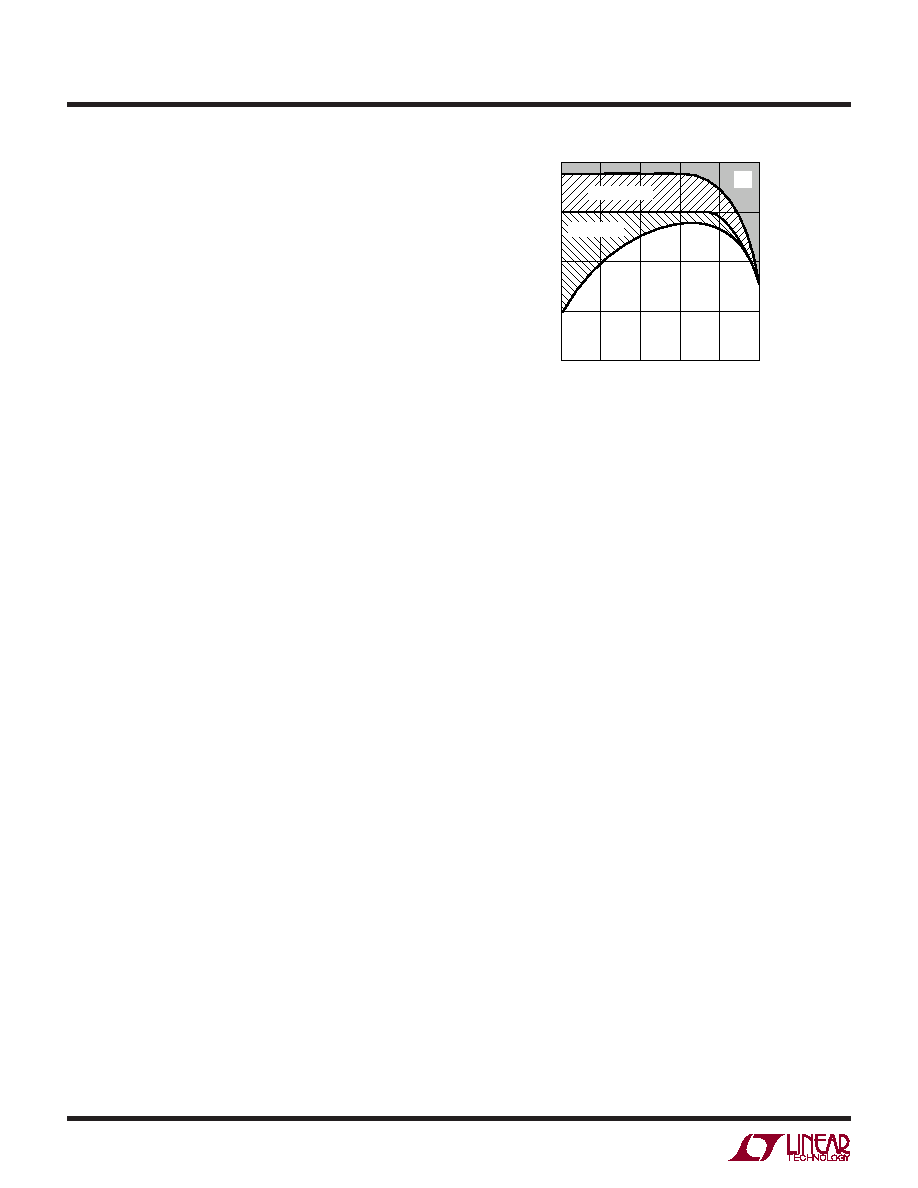
Figure 5 shows how the efficiency losses in a typical
LTC1148 series regulator end up being apportioned.
Figure 5. Efficiency Loss
OUTPUT CURRENT (A)
0.01
EFFICIENCY/LOSS
(%)
90
95
1
LTC1148 F05
85
80
0.03
0.1
0.3
3
100
GATE CHARGE
LTC1148 IQ
I2R
The gate charge loss is responsible for the majority of
the efficiency lost in the mid-current region. If Burst
Mode operation was not employed at low currents, the
gate charge loss alone would cause efficiency to drop to
unacceptable levels. With Burst Mode operation, the
DC supply current represents the lone (and unavoid-
able) loss component which continues to become a
higher percentage as output current is reduced. As
expected, the I2R losses dominate at high load currents.
Other losses including CIN and COUT ESR dissipative
losses, MOSFET switching losses, Schottky conduction
losses during dead time, and inductor core losses, gener-
ally account for less than 2% total additional loss.
Design Example
As a design example, assume VIN = 12V (nominal),
VOUT = 5V, IMAX = 2A, and f = 200kHz; RSENSE, CT and L
can immediately be calculated:
RSENSE = 100mV/2 = 0.05
tOFF = (1/200kHz)[1 – (5/12)] = 2.92s
CT = 2.92s/[(1.3)(104)] = 220pF
LMIN = 5.1(105)0.05(220pF)5V = 28H
Assume that the MOSFET dissipations are to be limited to
PN = PP = 250mW.
If TA = 50°C and the thermal resistance of each MOSFET
is 50°C/ W, then the junction temperatures will be 63°C
相关PDF资料 |
PDF描述 |
|---|---|
| LTC1148HVCS-5#TR | SWITCHING CONTROLLER, 250 kHz SWITCHING FREQ-MAX, PDSO14 |
| LTC1149CN-5#PBF | SWITCHING CONTROLLER, 250 kHz SWITCHING FREQ-MAX, PDIP16 |
| LTC1266CS#TR-3.3 | SWITCHING CONTROLLER, 400 kHz SWITCHING FREQ-MAX, PDSO16 |
| LTC1266IS#TR-3.3 | SWITCHING CONTROLLER, 400 kHz SWITCHING FREQ-MAX, PDSO16 |
| LTC1266IS#TR-5 | SWITCHING CONTROLLER, 400 kHz SWITCHING FREQ-MAX, PDSO16 |
相关代理商/技术参数 |
参数描述 |
|---|---|
| LTC1148HVCS5 | 制造商:LT 功能描述:REREALED |
| LTC1148HVCS-5 | 功能描述:IC REG CTRLR BUCK PWM CM 14-SOIC RoHS:否 类别:集成电路 (IC) >> PMIC - 稳压器 - DC DC 切换控制器 系列:- 标准包装:4,500 系列:PowerWise® PWM 型:控制器 输出数:1 频率 - 最大:1MHz 占空比:95% 电源电压:2.8 V ~ 5.5 V 降压:是 升压:无 回扫:无 反相:无 倍增器:无 除法器:无 Cuk:无 隔离:无 工作温度:-40°C ~ 125°C 封装/外壳:6-WDFN 裸露焊盘 包装:带卷 (TR) 配用:LM1771EVAL-ND - BOARD EVALUATION LM1771 其它名称:LM1771SSDX |
| LTC1148HVCS-5#PBF | 功能描述:IC REG CTRLR BUCK PWM CM 14-SOIC RoHS:是 类别:集成电路 (IC) >> PMIC - 稳压器 - DC DC 切换控制器 系列:- 标准包装:4,000 系列:- PWM 型:电压模式 输出数:1 频率 - 最大:1.5MHz 占空比:66.7% 电源电压:4.75 V ~ 5.25 V 降压:是 升压:无 回扫:无 反相:无 倍增器:无 除法器:无 Cuk:无 隔离:无 工作温度:-40°C ~ 85°C 封装/外壳:40-VFQFN 裸露焊盘 包装:带卷 (TR) |
| LTC1148HVCS-5#TR | 功能描述:IC REG CTRLR BUCK PWM CM 14-SOIC RoHS:否 类别:集成电路 (IC) >> PMIC - 稳压器 - DC DC 切换控制器 系列:- 标准包装:4,500 系列:PowerWise® PWM 型:控制器 输出数:1 频率 - 最大:1MHz 占空比:95% 电源电压:2.8 V ~ 5.5 V 降压:是 升压:无 回扫:无 反相:无 倍增器:无 除法器:无 Cuk:无 隔离:无 工作温度:-40°C ~ 125°C 封装/外壳:6-WDFN 裸露焊盘 包装:带卷 (TR) 配用:LM1771EVAL-ND - BOARD EVALUATION LM1771 其它名称:LM1771SSDX |
| LTC1148HVCS-5#TRPBF | 功能描述:IC REG CTRLR BUCK PWM CM 14-SOIC RoHS:是 类别:集成电路 (IC) >> PMIC - 稳压器 - DC DC 切换控制器 系列:- 标准包装:4,000 系列:- PWM 型:电压模式 输出数:1 频率 - 最大:1.5MHz 占空比:66.7% 电源电压:4.75 V ~ 5.25 V 降压:是 升压:无 回扫:无 反相:无 倍增器:无 除法器:无 Cuk:无 隔离:无 工作温度:-40°C ~ 85°C 封装/外壳:40-VFQFN 裸露焊盘 包装:带卷 (TR) |
发布紧急采购,3分钟左右您将得到回复。