- 您现在的位置:买卖IC网 > PDF目录2156 > LTC1150CS8#TRPBF (Linear Technology)IC OPAMP CHOP-STBL W/CAPS 8SOIC PDF资料下载
参数资料
| 型号: | LTC1150CS8#TRPBF |
| 厂商: | Linear Technology |
| 文件页数: | 2/16页 |
| 文件大小: | 0K |
| 描述: | IC OPAMP CHOP-STBL W/CAPS 8SOIC |
| 标准包装: | 2,500 |
| 放大器类型: | 断路器(零漂移) |
| 电路数: | 1 |
| 转换速率: | 3 V/µs |
| 增益带宽积: | 2.5MHz |
| 电流 - 输入偏压: | 10pA |
| 电压 - 输入偏移: | 0.5µV |
| 电流 - 电源: | 800µA |
| 电压 - 电源,单路/双路(±): | 4.75 V ~ 32 V,±2.38 V ~ 16 V |
| 工作温度: | 0°C ~ 70°C |
| 安装类型: | 表面贴装 |
| 封装/外壳: | 8-SOIC(0.154",3.90mm 宽) |
| 供应商设备封装: | 8-SO |
| 包装: | 带卷 (TR) |
LTC1150
10
1150fb
Table 1. Resistor Thermal EMF
RESISTOR TYPE
THERMAL EMF/°C GRADIENT
Tin Oxide
~mV/°C
Carbon Composition
~450V/°C
Metal Film
~20V/°C
WireWound
Evenohm
~2V/°C
Manganin
~2V/°C
PACKAGE-INDUCED OFFSET VOLTAGE
Package-induced thermal EMF effects are another impor-
tant source of errors. It arises at the copper/kovar
junctions formed when wire or printed circuit traces
contact a package lead. Like all the previously mentioned
thermal EMF effects, it is outside the LTC1150’s offset
nulling loop and cannot be cancelled. Metal can
H packages exhibit the worst warm-up drift. The input
offset voltage specification of the LTC1150 is actually set
by the package-induced warm-up drift rather than by the
circuit itself. The thermal time constant ranges from 0.5 to
3 minutes, depending on package type.
ALIASING
Like all sampled data systems, the LTC1150 exhibits
aliasing behavior at input frequencies near the sampling
frequency. The LTC1150 includes a high-frequency
correction loop which minimizes this effect; as a result,
aliasing is not a problem for most applications.
For a complete discussion of the correction circuitry and
aliasing behavior, please refer to the LTC1051/53 data
sheet.
SYNCHRONIZATION OF MULTIPLE LTC115O’S
When synchronization of several LTC1150’s is required,
one of the LTC1150’s can be used to provide the “master”
clock to control over 100 “slave” LTC1150’s. The master
clock, coming from Pin 8 of the master LTC1150, can
directly drive Pin 5 of the slaves. Note that Pin 8 of the slave
LTC1150’s will be pulled up to VS.
If all the LTC1150’s are to be synchronized with an external
clock, then the external clock should drive Pin 5 of all the
LTC1150’s.
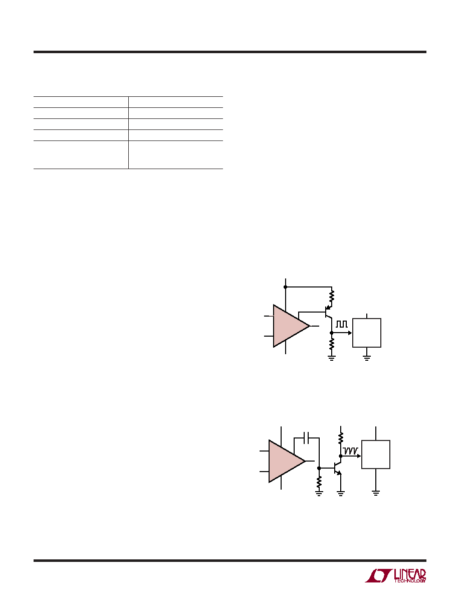
LEVEL SHIFTING THE CLOCK
Level shifting is needed if the clock output of the LTC1150
in ±15V operation must interface to regular 5V logic
circuits. Figures 2 and 3 show some typical level shifting
circuits.
When operated from single 5V or ±5V supplies, the
LTC1150 clock output at Pin 8 can interface to TTL or
CMOS inputs directly.
LOW SUPPLY OPERATION
The minimum supply for proper operation of the LTC1150
is typically below 4.0V (±2.0V). In single supply applica-
tions, PSRR is guaranteed down to 4.7V (±2.35V)
to ensure proper operation down to the minimum TTL
specified voltage of 4.75V.
Figure 2. Output Level Shift (Option 1)
Figure 3. Output Level Shift (Option 2)
LTC1150 AI02
10k
15V
–15V
5V
2
3
7
8
6
4
LTC1150
+
–
LOGIC
CIRCUIT
LTC1150 AI03
10k
100pF
GND
10k
15V
–15V
5V
2
3
7
8
6
4
LTC1150
+
–
LOGIC
CIRCUIT
APPLICATIO S I FOR ATIO
WU
UU
相关PDF资料 |
PDF描述 |
|---|---|
| LTC1151CSW | IC OPAMP ZERO-DRIFT DUAL 16SOIC |
| LTC1152CS8#TRPBF | IC OPAMP 0-DRFT R-R IN/OUT 8SOIC |
| LTC1992HMS8#TRPBF | IC AMP/DVR I/O FULLY DIFF 8-MSOP |
| LTC2050HVCS6#TRM | IC OPAMP ZERO-DRIFT SOT23-6 |
| LTC2051CDD | IC OPAMP ZERO-DRIFT DUAL 8DFN |
相关代理商/技术参数 |
参数描述 |
|---|---|
| LTC1150M | 制造商:LINER 制造商全称:Linear Technology 功能描述:+-15V Chopper Stabilized Operational Amplifier with Internal Capacitors |
| LTC1150MH | 制造商:未知厂家 制造商全称:未知厂家 功能描述:Chopper-Stabilized Operational Amplifier |
| LTC1150MJ/883 | 制造商:Linear Technology 功能描述: |
| LTC1150MJ8 | 制造商:Linear Technology 功能描述: |
| LTC1150MJ8/883 | 制造商:Linear Technology 功能描述:Precision Single Op Amp Single/Dual-Supply |
发布紧急采购,3分钟左右您将得到回复。