- 您现在的位置:买卖IC网 > PDF目录2156 > LTC1152CS8#TRPBF (Linear Technology)IC OPAMP 0-DRFT R-R IN/OUT 8SOIC PDF资料下载
参数资料
| 型号: | LTC1152CS8#TRPBF |
| 厂商: | Linear Technology |
| 文件页数: | 6/8页 |
| 文件大小: | 0K |
| 描述: | IC OPAMP 0-DRFT R-R IN/OUT 8SOIC |
| 标准包装: | 2,500 |
| 系列: | C-Load™ |
| 放大器类型: | 断路器(零漂移) |
| 电路数: | 1 |
| 输出类型: | 满摆幅 |
| 转换速率: | 0.5 V/µs |
| 增益带宽积: | 700kHz |
| 电流 - 输入偏压: | 10pA |
| 电压 - 输入偏移: | 1µV |
| 电流 - 电源: | 2.2mA |
| 电压 - 电源,单路/双路(±): | 2.7 V ~ 14 V,±1.35 V ~ 7 V |
| 工作温度: | 0°C ~ 70°C |
| 安装类型: | 表面贴装 |
| 封装/外壳: | 8-SOIC(0.154",3.90mm 宽) |
| 供应商设备封装: | 8-SO |
| 包装: | 带卷 (TR) |
6
LTC1152
U
S
A
O
PPLICATI
WU
U
I FOR ATIO
Rail-to-Rail Operation
The LTC1152 is a rail-to-rail input common-mode range,
rail-to-rail output swing op amp. Most CMOS op amps,
including the entire LTC zero-drift amplifier line, and even
a few bipolar op amps, can and do, claim rail-to-rail output
swing. One obvious use for such a device is to provide a
unity-gain buffer for 0V to 5V signals running from a single
5V power supply. This is not possible with the vast
majority of so-called “rail-to-rail” op amps; although the
output can swing to both rails, the negative input (which
is connected to the output) will exceed the common-mode
input range of the device at some point (generally about
1.5V below the positive supply), opening the feedback
loop and causing unpredictable and sometimes bizarre
behavior.
The LTC1152 is an exception to this rule. It features both
rail-to-rail output swing and rail-to-rail input common-
mode range (CMR); the input CMR actually extends be-
yond either rail by about 0.3V. This allows unity-gain
buffer circuits to operate with any input signal within the
power supply rails; input signal swing is limited only by the
output stage swing into the load. Additionally, signals
occurring at either rail (power supply current sensing, for
example) can be amplified without any special circuitry.
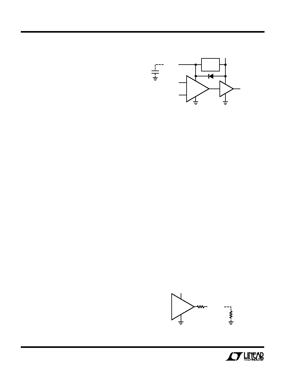
Internal Charge Pump
The LTC1152 achieves its rail-to-rail input CMR by using
a charge pump to generate an internal voltage approxi-
mately 2V higher than V+. The input stages of the op amp
are run from this higher voltage, making signals at V+
appear to be 2V below the front end’s power supply (Figure
1). The charge pump is contained entirely within the
LTC1152; no external components are required.
About 100
VP-P of residual charge pump switching noise
will be present on the output of the LTC1152. This
feedthrough is at 4.7MHz, higher than the gain-bandwidth
of the LTC1152, and will generally not cause any prob-
lems. Very sensitive applications can reduce this
feedthrough by connecting a capacitor from the CP pin
(pin 8) to V+(pin 7); a 0.1
F capacitor will reduce charge
pump feedthrough to negligible levels. The LTC1152 in-
cludes an internal diode from pin 8 to pin 7 to prevent
external parasitic capacitance from lengthening start-up
–
+
OUT
OUTPUT
RAIL TO RAIL
INPUT
0.1
F*
*OPTIONAL EXTERNAL
CAPACITOR TO REDUCE
CHARGE PUMP FEEDTHROUGH
VCC + 2V
VCC
(PIN 7)
CP (PIN 8)
+IN
–IN
1152 F01
INTERNAL
CHARGE
PUMP
Figure 1. LTC1152 Internal Block Diagram
time. This diode can stand short-term peak currents of
about 50mA, allowing it to quickly charge external capaci-
tance to ground or V –. Large capacitors (>1
F) should not
be connected between pin 8 and ground or V – to prevent
excessive diode current from flowing at start-up. The
LTC1152 can withstand continuous short circuits be-
tween pin 8 and V +; however, short circuiting pin 8 to
ground or V – will cause large amounts of current to flow
through the diode, destroying the LTC1152. Don’t do it.
Output Drive
The LTC1152 features an enhanced output stage that can
sink and source 10mA with a single 5V supply while
maintaining rail-to-rail output swing under most loading
conditions. The output stage can be modeled as a perfect
rail-to-rail voltage source with a resistor in series with it;
this open-loop output resistance limits the output swing
by creating a resistor divider with the output load.
The output resistance drops as total power supply voltage
increases, as shown in the typical performance curves. It
is typically 140
with a single 5V supply, allowing a 4.4V
output swing into a 1k resistor with a single 5V supply.
OUT (PIN 6)
≈140 AT 5V SUPPLY
LTC1152
OUTPUT
DRIVER
VCC (PIN 7)
RLOAD
ROUT
1152 F02
Figure 2. LTC1152 Output Resistance Model
相关PDF资料 |
PDF描述 |
|---|---|
| LTC1992HMS8#TRPBF | IC AMP/DVR I/O FULLY DIFF 8-MSOP |
| LTC2050HVCS6#TRM | IC OPAMP ZERO-DRIFT SOT23-6 |
| LTC2051CDD | IC OPAMP ZERO-DRIFT DUAL 8DFN |
| LTC2053HDD#TRPBF | IC AMP INST 0-DRFT R-R I/O 8-DFN |
| LTC2055HVIMS8#PBF | IC OPAMP ZERO DRFT DUAL LP 8MSOP |
相关代理商/技术参数 |
参数描述 |
|---|---|
| LTC1152I | 制造商:LINER 制造商全称:Linear Technology 功能描述:Rail-to-Rail Input Rail-to-Rail Output Zero-Drift Op Amp |
| LTC1152IN8 | 功能描述:IC OPAMP 0-DRFT R-R IN/OUT 8DIP RoHS:否 类别:集成电路 (IC) >> Linear - Amplifiers - Instrumentation 系列:C-Load™ 标准包装:1 系列:- 放大器类型:通用 电路数:4 输出类型:满摆幅 转换速率:0.028 V/µs 增益带宽积:105kHz -3db带宽:- 电流 - 输入偏压:3nA 电压 - 输入偏移:100µV 电流 - 电源:3.3µA 电流 - 输出 / 通道:12mA 电压 - 电源,单路/双路(±):2.7 V ~ 12 V,±1.35 V ~ 6 V 工作温度:-40°C ~ 85°C 安装类型:表面贴装 封装/外壳:14-TSSOP(0.173",4.40mm 宽) 供应商设备封装:14-TSSOP 包装:剪切带 (CT) 其它名称:OP481GRUZ-REELCT |
| LTC1152IN8#PBF | 功能描述:IC OPAMP 0-DRFT R-R IN/OUT 8DIP RoHS:是 类别:集成电路 (IC) >> Linear - Amplifiers - Instrumentation 系列:C-Load™ 标准包装:1 系列:- 放大器类型:通用 电路数:4 输出类型:满摆幅 转换速率:0.028 V/µs 增益带宽积:105kHz -3db带宽:- 电流 - 输入偏压:3nA 电压 - 输入偏移:100µV 电流 - 电源:3.3µA 电流 - 输出 / 通道:12mA 电压 - 电源,单路/双路(±):2.7 V ~ 12 V,±1.35 V ~ 6 V 工作温度:-40°C ~ 85°C 安装类型:表面贴装 封装/外壳:14-TSSOP(0.173",4.40mm 宽) 供应商设备封装:14-TSSOP 包装:剪切带 (CT) 其它名称:OP481GRUZ-REELCT |
| LTC1152IS8 | 功能描述:IC OPAMP 0-DRFT R-R IN/OUT 8SOIC RoHS:否 类别:集成电路 (IC) >> Linear - Amplifiers - Instrumentation 系列:C-Load™ 标准包装:73 系列:Over-The-Top® 放大器类型:通用 电路数:4 输出类型:满摆幅 转换速率:0.07 V/µs 增益带宽积:200kHz -3db带宽:- 电流 - 输入偏压:1nA 电压 - 输入偏移:285µV 电流 - 电源:50µA 电流 - 输出 / 通道:25mA 电压 - 电源,单路/双路(±):2 V ~ 44 V,±1 V ~ 22 V 工作温度:-40°C ~ 85°C 安装类型:表面贴装 封装/外壳:16-WFDFN 裸露焊盘 供应商设备封装:16-DFN-EP(5x3) 包装:管件 |
| LTC1152IS8#PBF | 功能描述:IC OPAMP 0-DRFT R-R IN/OUT 8SOIC RoHS:是 类别:集成电路 (IC) >> Linear - Amplifiers - Instrumentation 系列:C-Load™ 标准包装:2,500 系列:- 放大器类型:通用 电路数:4 输出类型:- 转换速率:0.6 V/µs 增益带宽积:1MHz -3db带宽:- 电流 - 输入偏压:45nA 电压 - 输入偏移:2000µV 电流 - 电源:1.4mA 电流 - 输出 / 通道:40mA 电压 - 电源,单路/双路(±):3 V ~ 32 V,±1.5 V ~ 16 V 工作温度:0°C ~ 70°C 安装类型:表面贴装 封装/外壳:14-TSSOP(0.173",4.40mm 宽) 供应商设备封装:14-TSSOP 包装:带卷 (TR) 其它名称:LM324ADTBR2G-NDLM324ADTBR2GOSTR |
发布紧急采购,3分钟左右您将得到回复。