- 您现在的位置:买卖IC网 > PDF目录15265 > LTC1159CG-3.3#PBF (Linear Technology)IC REG CTRLR BUCK PWM CM 20-SSOP PDF资料下载
参数资料
| 型号: | LTC1159CG-3.3#PBF |
| 厂商: | Linear Technology |
| 文件页数: | 11/20页 |
| 文件大小: | 0K |
| 描述: | IC REG CTRLR BUCK PWM CM 20-SSOP |
| 标准包装: | 66 |
| PWM 型: | 电流模式 |
| 输出数: | 1 |
| 频率 - 最大: | 250kHz |
| 占空比: | 100% |
| 电源电压: | 4 V ~ 40 V |
| 降压: | 是 |
| 升压: | 无 |
| 回扫: | 无 |
| 反相: | 无 |
| 倍增器: | 无 |
| 除法器: | 无 |
| Cuk: | 无 |
| 隔离: | 无 |
| 工作温度: | 0°C ~ 70°C |
| 封装/外壳: | 20-SSOP(0.209",5.30mm 宽) |
| 包装: | 管件 |
�� �
�
�LTC1159�
�LTC1159-3.3/LTC1159-5�
�APPLICATIO� S� I� FOR� ATIO�
�discharged� bypass� capacitors� are� effectively� put� in� parallel�
�with� C� OUT� ,� causing� a� rapid� drop� in� V� OUT� .� No� regulator� can�
�deliver� enough� current� to� prevent� this� problem� if� the� load�
�switch� resistance� is� low� and� it� is� driven� quickly.� The� only�
�solution� is� to� limit� the� rise� time� of� the� switch� drive� so� that�
�the� load� rise� time� is� limited� to� approximately� 25� ?� C� LOAD� .�
�Thus� a� 10� μ� F� capacitor� would� require� a� 250� μ� s� rise� time,�
�limiting� the� charging� current� to� about� 200mA.�
�Line� Transient� Response�
�The� LTC1159� has� better� than� 60dB� line� rejection� and� is�
�generally� impervious� to� large� positive� or� negative� line�
�voltage� transients.� However,� one� rarely� occurring� condi-�
�tion� can� cause� the� output� voltage� to� overshoot� if� the� proper�
�precautions� are� not� observed.� This� condition� is� a� negative�
�V� IN� transition� of� several� volts� followed� within� 100� μ� s� by� a�
�positive� transition� of� greater� than� 0.5V/� μ� s� slew� rate.�
�The� reason� this� condition� rarely� occurs� is� because� it� takes�
�tens� of� amps� to� slew� the� regulator� input� capacitor� at� this�
�rate!� The� solution� is� to� add� a� diode� between� the� cap� and� V� IN�
�pins� of� the� LTC1159� as� shown� in� several� of� the� typical�
�application� circuits.� If� you� think� your� system� could� have�
�this� problem,� add� the� diode.� Note� that� in� surface� mount�
�applications� it� can� be� combined� with� the� P-gate� diode� by�
�using� a� low� cost� common� cathode� dual� diode.�
�EXTV� CC� Pin� Connection�
�The� LTC1159� contains� an� internal� PNP� switch� connected�
�between� the� EXTV� CC� and� V� CC� pins.� The� switch� closes� and�
�supplies� the� V� CC� power� whenever� the� EXTV� CC� pin� is� higher�
�in� voltage� than� the� 4.5V� internal� regulator.� This� allows� the�
�V� IN�
�MOSFET� driver� and� control� power� to� be� derived� from� the�
�output� during� normal� operation� and� from� the� internal�
�regulator� when� the� output� is� out� of� regulation� (start-up,�
�short� circuit).�
�Significant� efficiency� gains� can� be� realized� by� powering� V� CC�
�from� the� output,� since� the� V� IN� current� resulting� from� the�
�driver� and� control� currents� will� be� scaled� by� a� factor� of�
�(Duty� Cycle)/(Efficiency).� For� 5V� regulators� this� simply�
�means� connecting� the� EXTV� CC� pin� directly� to� V� OUT� .� How-�
�ever,� for� 3.3V� and� other� low� voltage� regulators,� additional�
�circuitry� is� required� to� derive� V� CC� power� from� the� output.�
�The� following� list� summarizes� the� four� possible� connec-�
�tions� for� EXTV� CC� :�
�1.� EXTV� CC� Left� Open.� This� will� cause� V� CC� to� be� powered�
�only� from� the� internal� 4.5V� regulator� resulting� in� reduced�
�MOSFET� gate� drive� levels� and� an� efficiency� penalty� of� up� to�
�10%� at� high� input� voltages.�
�2.� EXTV� CC� Connected� Directly� to� V� OUT� .� This� is� the� normal�
�connection� for� a� 5V� regulator� and� provides� the� highest�
�efficiency.�
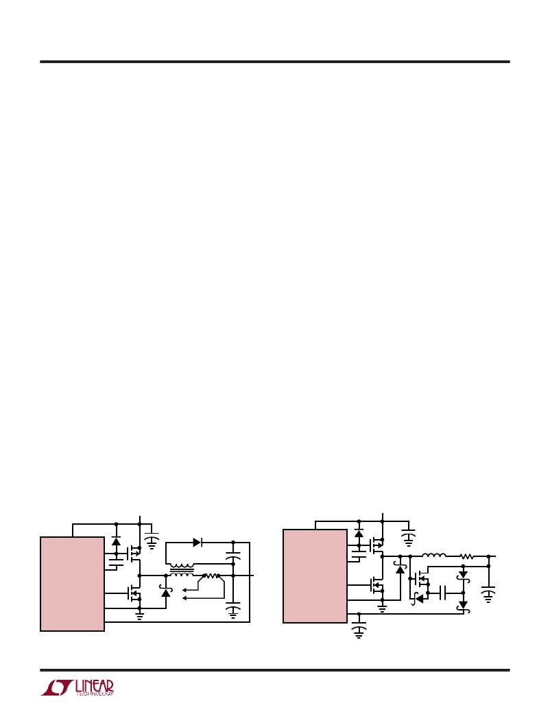
�3.� EXTV� CC� Connected� to� an� Output-Derived� Boost� Net-�
�work.� For� 3.3V� and� other� low� voltage� regulators,� efficiency�
�gains� can� still� be� realized� by� connecting� EXTV� CC� to� an�
�output-derived� voltage� which� has� been� boosted� to� greater�
�than� 4.5V.� This� can� be� done� either� with� the� inductive� boost�
�winding� shown� in� Figure� 5a� or� the� capacitive� charge� pump�
�shown� in� Figure� 5b.� The� charge� pump� has� the� advantage� of�
�simple� magnetics� and� generally� provides� the� highest� effi-�
�ciency� at� the� expense� of� a� slightly� higher� parts� count.�
�V� IN�
�V� IN�
�P-GATE�
�+�
�P-CH�
�C� IN�
�L�
�1:1�
�BAT85�
�?�
�1� μ� F�
�+�
�V� IN�
�P-GATE�
�P-DRIVE�
�P-CH�
�+�
�C� IN�
�L�
�R� SENSE�
�V� OUT�
�R� SENSE�
�P-DRIVE�
�LTC1159-3.3�
�N-GATE�
�P-GND�
�EXTV� CC�
�N-CH�
�?�
�3�
�1�
�2�
�C� OUT�
�4�
�+�
�LTC1159� ?� F05a�
�V� OUT�
�LTC1159-3.3�
�N-GATE�
�P-GND�
�EXTV� CC�
�+�
�1� μ� F�
�N-CH�
�BAT85�
�VN2222LL�
�0.22� μ� F�
�LTC1159� ?� F05b�
�BAT85�
�+�
�BAT85�
�C� OUT�
�Figure� 5a.� Inductive� Boost� Circuit� for� EXTV� CC�
�Figure� 5b.� Capacitive� Charge� Pump� for� EXTV� CC�
�11�
�相关PDF资料 |
PDF描述 |
|---|---|
| LTC1159CG-3.3 | IC REG CTRLR BUCK PWM CM 20-SSOP |
| H2AXT-10112-V4-ND | JUMPER-H1502TR/A2015V/X 12" |
| LTC1159CG#PBF | IC REG CTRLR BUCK PWM CM 20-SSOP |
| ESM06DRMD-S273 | CONN EDGECARD 12POS .156 WW |
| LTC1159CG | IC REG CTRLR BUCK PWM CM 20-SSOP |
相关代理商/技术参数 |
参数描述 |
|---|---|
| LTC1159CG-5 | 功能描述:IC REG CTRLR BUCK PWM CM 20-SSOP RoHS:否 类别:集成电路 (IC) >> PMIC - 稳压器 - DC DC 切换控制器 系列:- 标准包装:4,500 系列:PowerWise® PWM 型:控制器 输出数:1 频率 - 最大:1MHz 占空比:95% 电源电压:2.8 V ~ 5.5 V 降压:是 升压:无 回扫:无 反相:无 倍增器:无 除法器:无 Cuk:无 隔离:无 工作温度:-40°C ~ 125°C 封装/外壳:6-WDFN 裸露焊盘 包装:带卷 (TR) 配用:LM1771EVAL-ND - BOARD EVALUATION LM1771 其它名称:LM1771SSDX |
| LTC1159CG-5#PBF | 功能描述:IC REG CTRLR BUCK PWM CM 20-SSOP RoHS:是 类别:集成电路 (IC) >> PMIC - 稳压器 - DC DC 切换控制器 系列:- 标准包装:4,000 系列:- PWM 型:电压模式 输出数:1 频率 - 最大:1.5MHz 占空比:66.7% 电源电压:4.75 V ~ 5.25 V 降压:是 升压:无 回扫:无 反相:无 倍增器:无 除法器:无 Cuk:无 隔离:无 工作温度:-40°C ~ 85°C 封装/外壳:40-VFQFN 裸露焊盘 包装:带卷 (TR) |
| LTC1159CG-5#TR | 功能描述:IC REG CTRLR BUCK PWM CM 20-SSOP RoHS:否 类别:集成电路 (IC) >> PMIC - 稳压器 - DC DC 切换控制器 系列:- 标准包装:4,500 系列:PowerWise® PWM 型:控制器 输出数:1 频率 - 最大:1MHz 占空比:95% 电源电压:2.8 V ~ 5.5 V 降压:是 升压:无 回扫:无 反相:无 倍增器:无 除法器:无 Cuk:无 隔离:无 工作温度:-40°C ~ 125°C 封装/外壳:6-WDFN 裸露焊盘 包装:带卷 (TR) 配用:LM1771EVAL-ND - BOARD EVALUATION LM1771 其它名称:LM1771SSDX |
| LTC1159CG-5#TRPBF | 功能描述:IC REG CTRLR BUCK PWM CM 20-SSOP RoHS:是 类别:集成电路 (IC) >> PMIC - 稳压器 - DC DC 切换控制器 系列:- 标准包装:4,000 系列:- PWM 型:电压模式 输出数:1 频率 - 最大:1.5MHz 占空比:66.7% 电源电压:4.75 V ~ 5.25 V 降压:是 升压:无 回扫:无 反相:无 倍增器:无 除法器:无 Cuk:无 隔离:无 工作温度:-40°C ~ 85°C 封装/外壳:40-VFQFN 裸露焊盘 包装:带卷 (TR) |
| LTC1159CN | 制造商:LINER 制造商全称:Linear Technology 功能描述:High Efficiency Synchronous Step-Down Switching Regulators |
发布紧急采购,3分钟左右您将得到回复。