- 您现在的位置:买卖IC网 > PDF目录11022 > LTC1164-6CN (Linear Technology)IC FILTR 8TH ORDER LOWPASS 14DIP PDF资料下载
参数资料
| 型号: | LTC1164-6CN |
| 厂商: | Linear Technology |
| 文件页数: | 10/12页 |
| 文件大小: | 0K |
| 描述: | IC FILTR 8TH ORDER LOWPASS 14DIP |
| 标准包装: | 25 |
| 滤波器类型: | 椭圆或贝塞尔低通 |
| 频率 - 截止或中心: | 30kHz |
| 滤波器数: | 1 |
| 滤波器阶数: | 8th |
| 电源电压: | 4.75 V ~ 16 V,±2.375 V ~ 8 V |
| 安装类型: | 通孔 |
| 封装/外壳: | 14-DIP(0.300",7.62mm) |
| 供应商设备封装: | 14-PDIP |
| 包装: | 管件 |
7
LTC1164-6
11646fa
PI FU CTIO S
U
UU
(14-Lead Dual-In-Line Package)
buffer, Figure 3,can be used provided that its input common
mode range is well within the filter’s output swing. Pin 6 is
an intermediate filter output providing an unspecified 6th
order lowpass filter. Pin 6 should not be loaded.
ELLIPTIC/LINEAR PHASE (Pin 10): The DC level at this pin
selects the desired filter response, elliptic or linear phase
and determines the ratio of the clock frequency to the
cutoff frequency of the filter. Pin 10 connected to V –
provides an elliptic lowpass filter with clock-to-fCUTOFF
ratio of 100:1. Pin 10 connected to analog ground pro-
vides a linear phase lowpass filter with a clock- to-f–3dB
ratio of 160:1 and a transient response overshoot of 1%.
When Pin 10 is connected to V+ the clock-to-fCUTOFF ratio
is 50:1 and the filter response is elliptic. Bypassing Pin 10
to analog ground reduces the output DC offsets. If the DC
level at Pin 10 is switched mechanically or electrically at
slew rates greater than 1V/
swhilethedeviceisoperating,
a 10k resistor should be connected between Pin 10 and the
DC source.
CLK (Pin 11): Any TTL or CMOS clock source with a
square-wave output and 50% duty cycle (
±10%) is an
adequate clock source for the device. The power supply for
the clock source should not be the filter’s power supply.
The analog ground for the filter should be connected to
clock’s ground at a single point only. Table 1 shows the
clock’s low and high level threshold value for a dual or
single supply operation. A pulse generator can be used as
a clock source provided the high level ON time is greater
than 0.5
s. Sine waves are not recommended for clock
input frequencies less than 100kHz, since excessively
slow clock rise or fall times generate internal clock jitter
(maximum clock rise or fall time
≤ 1s). The clock signal
should be routed from the right side of the IC package to
avoid coupling into any input or output analog signal path.
A 1k resistor between clock source and Pin 11 will slow
down the rise and fall times of the clock to further reduce
charge coupling, Figures 1 and 2.
1k
1164-6 F03
–
+
LT1006, fC < 5kHz
LT1200, fC > 5kHz
Figure 3. Buffer for Filter Output
V– (Pins 7, 14): Pins 7 and 14 should be connected
together. In a printed circuit board the connection should
be done under the IC package through a short trace
surrounded by the analog ground plane.
VOUT (Pins 9, 6): Pin 9 is the specified output of the filter;
it can typically source or sink 1mA. Driving coaxial cables
or resistive loads less than 20k will degrade the total
harmonicdistortionofthefilter.Whenevaluatingthedevice’s
distortion an output buffer is required. A noninverting
could go above ground, a signal diode must be used to
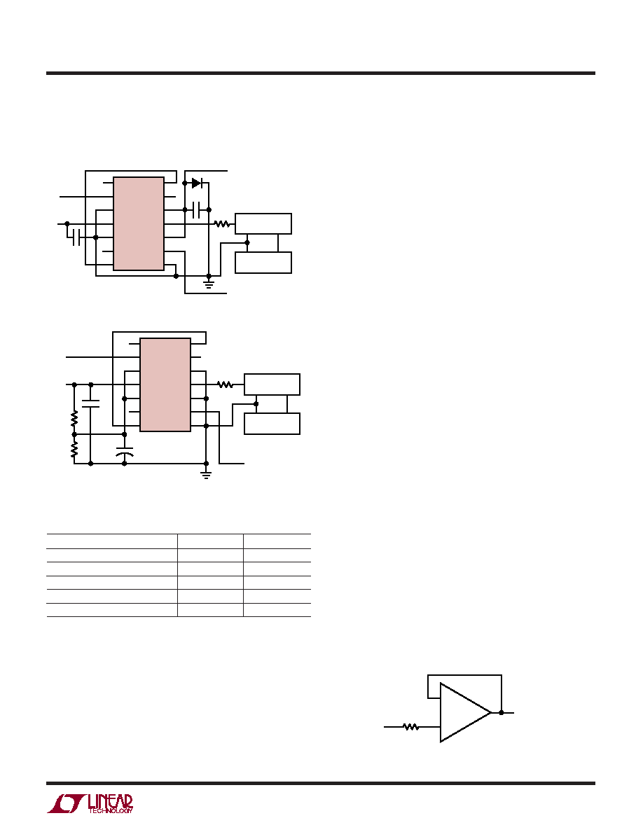
clamp V. Figures 1 and 2 show typical connections for dual
and single supply operation.
1
2
3
4
5
6
7
14
13
12
11
10
9
8
VIN
V+
1k
V–
VOUT
LTC1164-6
DIGITAL SUPPLY
+
GND
CLOCK SOURCE
*
1164-6 F01
* OPTIONAL
0.1
F
0.1
F
Figure 1. Dual Supply Operation for fCLK/fCUTOFF = 100:1
Table 1. Clock Source High and Low Threshold Levels
POWER SUPPLY
HIGH LEVEL
LOW LEVEL
Dual Supply =
±7.5V
≥ 2.18V
≤ 0.5V
Dual Supply =
±5V
≥ 1.45V
≤ 0.5V
Dual Supply =
±2.5V
≥ 0.73V
≤ – 2.0V
Single Supply = 12V
≥ 7.80V
≤ 6.5V
Single Supply = 5V
≥ 1.45V
≤ 0.5V
Figure 2. Single Supply Operation for fCLK/fCUTOFF = 100:1
1
2
3
4
5
6
7
14
13
12
11
10
9
8
VIN
V+
1k
VOUT
DIGITAL SUPPLY
+
GND
CLOCK SOURCE
1164-6 F02
+
LTC1164-6
0.1
F
1
F
10k
相关PDF资料 |
PDF描述 |
|---|---|
| LTC1562ACG#TR | IC FILTER UNIV RC QUAD LN 20SSOP |
| LTC1562ACG#PBF | IC FILTER UNIV RC QUAD LN 20SSOP |
| LTC1562ACG | IC FILTER UNIVRSL RC QUAD 20SSOP |
| LTC1562ACG#TRPBF | IC FILTER UNIV RC QUAD LN 20SSOP |
| MC9S08QB8CTGR | IC MCU 8K FLASH 16-TSSOP |
相关代理商/技术参数 |
参数描述 |
|---|---|
| LTC1164-6CN#PBF | 功能描述:IC FILTR 8TH ORDER LOWPASS 14DIP RoHS:是 类别:集成电路 (IC) >> 接口 - 滤波器 - 有源 系列:- 产品培训模块:Lead (SnPb) Finish for COTS Obsolescence Mitigation Program 标准包装:1,000 系列:- 滤波器类型:连续时间,带通低通 频率 - 截止或中心:150kHz 滤波器数:4 滤波器阶数:8th 电源电压:4.74 V ~ 11 V,±2.37 V ~ 5.5 V 安装类型:表面贴装 封装/外壳:28-SOIC(0.295",7.50mm 宽) 供应商设备封装:28-SOIC W 包装:带卷 (TR) |
| LTC1164-6CS | 制造商:LINER 制造商全称:Linear Technology 功能描述:Low Power 8th Order Pin Selectable Elliptic or Linear Phase Lowpass Filter |
| LTC1164-6CSW | 功能描述:IC FILTR 8TH ORDR LOWPASS 16SOIC RoHS:否 类别:集成电路 (IC) >> 接口 - 滤波器 - 有源 系列:- 产品培训模块:Lead (SnPb) Finish for COTS Obsolescence Mitigation Program 标准包装:1,000 系列:- 滤波器类型:连续时间,带通低通 频率 - 截止或中心:150kHz 滤波器数:4 滤波器阶数:8th 电源电压:4.74 V ~ 11 V,±2.37 V ~ 5.5 V 安装类型:表面贴装 封装/外壳:28-SOIC(0.295",7.50mm 宽) 供应商设备封装:28-SOIC W 包装:带卷 (TR) |
| LTC1164-6CSW#PBF | 功能描述:IC FILTR 8TH ORDR LOWPASS 16SOIC RoHS:是 类别:集成电路 (IC) >> 接口 - 滤波器 - 有源 系列:- 产品培训模块:Lead (SnPb) Finish for COTS Obsolescence Mitigation Program 标准包装:1,000 系列:- 滤波器类型:连续时间,带通低通 频率 - 截止或中心:150kHz 滤波器数:4 滤波器阶数:8th 电源电压:4.74 V ~ 11 V,±2.37 V ~ 5.5 V 安装类型:表面贴装 封装/外壳:28-SOIC(0.295",7.50mm 宽) 供应商设备封装:28-SOIC W 包装:带卷 (TR) |
| LTC1164-6CSW#TR | 功能描述:IC FILTER LP 8TH ORDER 16SOIC RoHS:否 类别:集成电路 (IC) >> 接口 - 滤波器 - 有源 系列:- 产品培训模块:Lead (SnPb) Finish for COTS Obsolescence Mitigation Program 标准包装:1,000 系列:- 滤波器类型:连续时间,带通低通 频率 - 截止或中心:150kHz 滤波器数:4 滤波器阶数:8th 电源电压:4.74 V ~ 11 V,±2.37 V ~ 5.5 V 安装类型:表面贴装 封装/外壳:28-SOIC(0.295",7.50mm 宽) 供应商设备封装:28-SOIC W 包装:带卷 (TR) |
发布紧急采购,3分钟左右您将得到回复。