- 您现在的位置:买卖IC网 > PDF目录10339 > LTC1197IMS8#TR (Linear Technology)IC ADC 10BIT 500KHZ SHTDWN 8MSOP PDF资料下载
参数资料
| 型号: | LTC1197IMS8#TR |
| 厂商: | Linear Technology |
| 文件页数: | 8/28页 |
| 文件大小: | 0K |
| 描述: | IC ADC 10BIT 500KHZ SHTDWN 8MSOP |
| 标准包装: | 2,500 |
| 位数: | 10 |
| 采样率(每秒): | 500k |
| 数据接口: | MICROWIRE?,串行,SPI? |
| 转换器数目: | 1 |
| 功率耗散(最大): | 25mW |
| 电压电源: | 单电源 |
| 工作温度: | -40°C ~ 85°C |
| 安装类型: | 表面贴装 |
| 封装/外壳: | 8-TSSOP,8-MSOP(0.118",3.00mm 宽) |
| 供应商设备封装: | 8-MSOP |
| 包装: | 带卷 (TR) |
| 输入数目和类型: | 1 个差分,单极 |
第1页第2页第3页第4页第5页第6页第7页当前第8页第9页第10页第11页第12页第13页第14页第15页第16页第17页第18页第19页第20页第21页第22页第23页第24页第25页第26页第27页第28页
16
LTC1197/LTC1197L
LTC1199/LTC1199L
Mixed Supplies
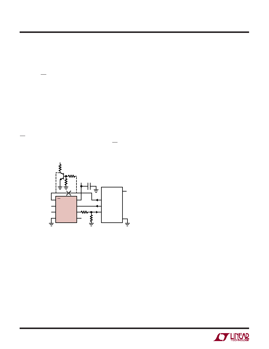
It is possible to have a microprocessor running off a 5V
supply and communicate with the ADC operating on 3V or
9V supplies. The requirement to achieve this is that the
outputs of CS, CLK and DIN from the MPU have to be able
to trip the equivalent inputs of the ADC and the output of
the ADC must be able to toggle the equivalent input of the
MPU (see typical curve of Digital Input Logic Threshold vs
Supply Voltage). With the LTC1197 operating on a 9V
supply, the output of DOUT may go between 0V and 9V. The
9V output may damage the MPU running off a 5V supply.
The way to solve this problem is to have a resistor divider
on DOUT (Figure 4) and connect the center point to the
MPU input. It should be noted that to get full shutdown, the
CS input of the ADC must be driven to the VCC voltage. This
would require adding a level shift circuit to the CS signal
in Figure 4.
SAMPLE-AND-HOLD
The LTC1197/LTC1197L/LTC1199/LTC1199L provide a
built-in sample-and-hold (S /H) function to acquire sig-
nals. The S /H of the LTC1197/LTC1197L acquires input
signals for the “+” input relative to the “–” input during the
tSMPL time(seeFigure1).HowevertheS /HoftheLTC1199/
LTC1199L can sample input signals from the “+” input
relative to ground and from the “–” input relative to ground
in addition to acquiring signals from the “+” input relative
to the “–” input (see Figure 5) during tSMPL.
Single-Ended Inputs
The sample-and-hold of the LTC1199/LTC1199L allows
conversion of rapidly varying signals. The input voltage is
sampled during the tSMPL time as shown in Figure 5. The
sampling interval begins as the ODD/SGN bit is shifted in
and continues until the falling CLK edge after the dummy
bit is received. On this falling edge, the S/H goes into hold
mode and the conversion begins.
Differential Inputs
With differential inputs, the ADC no longer converts just a
single voltage but rather the difference between two volt-
ages. In this case, the voltage on the selected “+” input is
still sampled and held and therefore may be rapidly time
varying just as in single-ended mode. However, the volt-
age on the selected “–” input must remain constant and be
free of noise and ripple throughout the conversion time.
Otherwise, the differencing operation may not be per-
formed accurately. The conversion time is 10.5 CLK cycles.
Therefore, a change in the “–” input voltage during this
interval can cause conversion errors. For a sinusoidal
voltage on the “–” input this error would be:
VERROR (MAX) = VPEAK 2 π f(“–”) 10.5/fCLK
Where f(“–”) is the frequency of the “–” input voltage,
VPEAK is its peak amplitude and fCLK is the frequency of the
CLK. In most cases VERROR will not be significant. For a
60Hz signal on the “–” input to generate a 1/4LSB error
(1.22mV) with the converter running at CLK = 7.2MHz, its
peak value would have to be 2.22V.
Figure 4. Interfacing a 9V-Powered LTC1197 to a 5V System
BOARD LAYOUT CONSIDERATIONS
Grounding and Bypassing
The LTC1197/LTC1197L/LTC1199/LTC1199L should be
used with an analog ground plane and single point ground-
ing techniques. The GND pin should be tied directly to the
ground plane. The VCC pin should be bypassed to the
ground plane using a 1
F tantalum capacitor with leads as
short as possible. All analog inputs should be referenced
directly to the single point ground. Digital inputs and
outputs should be shielded from and/or routed away from
the reference and analog circuitry.
APPLICATIO S I FOR ATIO
WU
UU
+IN
–IN
GND
VCC
CLK
DOUT
VREF
4.7k
6V
4.7
F
MPU
(e.g. 8051)
5V
P1.4
P1.3
P1.2
1197/99 F04
DIFFERENTIAL INPUTS
COMMON MODE RANGE
0V TO 6V
9V
LTC1197
9V
OPTIONAL
LEVEL SHIFT
CS
相关PDF资料 |
PDF描述 |
|---|---|
| LTC2305IMS#TRPBF | IC ADC 12-BIT 2CHN 12-MSOP |
| LTC2305IDE#TRPBF | IC ADC 12-BIT 2CHN 12-DFN |
| LTC2306IDD#TRPBF | IC ADC 12-BIT 2CH 500KSPS 10DFN |
| LTC2302IDD#TRPBF | IC ADC 12-BIT 1CH 500KSPS 10DFN |
| MAX9789BETJ+ | IC AMP AUDIO 2W STER AB 32TQFN |
相关代理商/技术参数 |
参数描述 |
|---|---|
| LTC1197IS8 | 功能描述:IC A/DCONV 10BIT W/SHTDWN 8-SOIC RoHS:否 类别:集成电路 (IC) >> 数据采集 - 模数转换器 系列:- 标准包装:2,500 系列:- 位数:16 采样率(每秒):15 数据接口:MICROWIRE?,串行,SPI? 转换器数目:1 功率耗散(最大):480µW 电压电源:单电源 工作温度:-40°C ~ 85°C 安装类型:表面贴装 封装/外壳:38-WFQFN 裸露焊盘 供应商设备封装:38-QFN(5x7) 包装:带卷 (TR) 输入数目和类型:16 个单端,双极;8 个差分,双极 配用:DC1011A-C-ND - BOARD DELTA SIGMA ADC LTC2494 |
| LTC1197IS8#PBF | 功能描述:IC A/DCONV 10BIT W/SHTDWN 8-SOIC RoHS:是 类别:集成电路 (IC) >> 数据采集 - 模数转换器 系列:- 标准包装:1 系列:microPOWER™ 位数:8 采样率(每秒):1M 数据接口:串行,SPI? 转换器数目:1 功率耗散(最大):- 电压电源:模拟和数字 工作温度:-40°C ~ 125°C 安装类型:表面贴装 封装/外壳:24-VFQFN 裸露焊盘 供应商设备封装:24-VQFN 裸露焊盘(4x4) 包装:Digi-Reel® 输入数目和类型:8 个单端,单极 产品目录页面:892 (CN2011-ZH PDF) 其它名称:296-25851-6 |
| LTC1197IS8#TR | 功能描述:IC ADC 10BIT 500KHZ SHTDWN 8SOIC RoHS:否 类别:集成电路 (IC) >> 数据采集 - 模数转换器 系列:- 标准包装:2,500 系列:- 位数:16 采样率(每秒):15 数据接口:MICROWIRE?,串行,SPI? 转换器数目:1 功率耗散(最大):480µW 电压电源:单电源 工作温度:-40°C ~ 85°C 安装类型:表面贴装 封装/外壳:38-WFQFN 裸露焊盘 供应商设备封装:38-QFN(5x7) 包装:带卷 (TR) 输入数目和类型:16 个单端,双极;8 个差分,双极 配用:DC1011A-C-ND - BOARD DELTA SIGMA ADC LTC2494 |
| LTC1197IS8#TRPBF | 功能描述:IC A/DCONV 10BIT W/SHTDWN 8-SOIC RoHS:是 类别:集成电路 (IC) >> 数据采集 - 模数转换器 系列:- 标准包装:2,500 系列:- 位数:16 采样率(每秒):15 数据接口:MICROWIRE?,串行,SPI? 转换器数目:1 功率耗散(最大):480µW 电压电源:单电源 工作温度:-40°C ~ 85°C 安装类型:表面贴装 封装/外壳:38-WFQFN 裸露焊盘 供应商设备封装:38-QFN(5x7) 包装:带卷 (TR) 输入数目和类型:16 个单端,双极;8 个差分,双极 配用:DC1011A-C-ND - BOARD DELTA SIGMA ADC LTC2494 |
| LTC1197L | 制造商:LINER 制造商全称:Linear Technology 功能描述:10-Bit, 500ksps ADCs in MSOP with Auto Shutdown |
发布紧急采购,3分钟左右您将得到回复。