- 您现在的位置:买卖IC网 > PDF目录2003 > LTC1257IS8#TRPBF (Linear Technology)IC D/A CONV 12BIT VOLT OUT 8SOIC PDF资料下载
参数资料
| 型号: | LTC1257IS8#TRPBF |
| 厂商: | Linear Technology |
| 文件页数: | 9/12页 |
| 文件大小: | 0K |
| 描述: | IC D/A CONV 12BIT VOLT OUT 8SOIC |
| 标准包装: | 2,500 |
| 设置时间: | 6µs |
| 位数: | 12 |
| 数据接口: | 串行 |
| 转换器数目: | 1 |
| 电压电源: | 单电源 |
| 功率耗散(最大): | 1.75mW |
| 工作温度: | -40°C ~ 85°C |
| 安装类型: | 表面贴装 |
| 封装/外壳: | 8-SOIC(0.154",3.90mm 宽) |
| 供应商设备封装: | 8-SOIC |
| 包装: | 带卷 (TR) |
| 输出数目和类型: | 1 电压,单极 |
| 采样率(每秒): | * |
LTC1257
6
1257fc
PIN FUNCTIONS
DEFINITIONS
VOUT (Pin 7): The buffered DAC output is capable of
sourcing 2mA over temperature while pulling within 2.7V
of VCC. The output will pull to ground through an internal
250Ω equivalent resistance.
VCC (Pin 8): The positive supply input. 4.75V ≤ VCC ≤
15.75V. Requires a bypass capacitor to ground.
LSB: The least significant bit or the ideal voltage difference
between two successive codes.
LSB = (VFS – VOS)/2n – 1
n
= The number of digital input bits
VOS = The zero code error or offset of the DAC
VFS = The full-scale output voltage of the DAC
measured when all bits are set to 1
Resolution: The resolution is the number of DAC output
states (2n) that divide the full-scale range. The resolution
does not imply linearity.
INL:End-pointintegralnonlinearityisthemaximumdevia-
tion from a straight line passing through the end-points of
the DAC transfer curve. Because the part operates from
a single supply and the output cannot go below ground,
the linearity is measured between full-scale and the first
code that guarantees a positive output. The INL error at
a given input code is calculated as follows:
INL
= (VOUT – VIDEAL)/LSB
VIDEAL = (Code)(LSB) + VOS
VOUT = The output voltage of the DAC measured at
the given input code
DNL: Differential nonlinearity is the difference between
the measured change and the ideal 1LSB change between
any two adjacent codes. The DNL error between any two
codes is calculated as follows:
DNL = (VOUT – LSB)/LSB
VOUT= The measured voltage difference between two
adjacent codes
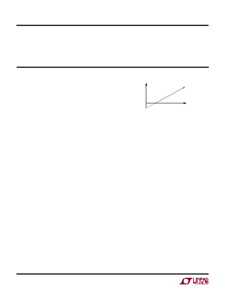
Offset Error: The theoretical voltage at the output when
the DAC is loaded with all zeros. The output amplifier can
have a true negative offset, but because the part is oper-
ated from a single supply, the output cannot go below
ground. If the offset is negative, the output will remain
near 0V resulting in the transfer curve shown in Figure 1.
The offset of the part is measured at the first code that
produces an output voltage 0.5LSB greater than the
previous code:
VOS = VOUT – [(Code)(VFS)/(2n – 1)]
Full-Scale Error: Full-scale error is the difference between
the ideal and measured DAC output voltages with all bits
set to one (Code = 4095). The full-scale error includes the
offset error and is calculated as follows:
FSE = (VOUT – VIDEAL)/LSB
VIDEAL = (VREF)(1 – 2–n) – VOS
VREF =Thereferencevoltage,eitherinternalorexternal
Gain Error: Gain error is the difference between the ideal
and measured slope of the DAC transfer characteristic.
Gain error is equal to full-scale error minus offset error.
Digital Feedthrough: The glitch that appears at the analog
output caused by AC coupling from the digital inputs when
they change state. The area of the glitch is specified in
(nV)(sec).
OUTPUT
VOLTAGE
NEGATIVE
OFFSET
{
DAC CODE
0V
1257 F01
Figure 1. Effect of Negative Offset
相关PDF资料 |
PDF描述 |
|---|---|
| LTC1276ACN#PBF | IC A/D CONV 12BIT SAMPLING 24DIP |
| LTC1278-4IN#PBF | IC A/DCONV SAMPLNG W/SHTDN 24DIP |
| LTC1279CG#TRPBF | IC A/DCONV SAMPLNG W/SHTDN24SSOP |
| LTC1282ACN#PBF | IC A/D CONV SAMPLING W/REF 24DIP |
| LTC1288IS8#TRPBF | IC A/D CONV SAMPLING 12BIT 8SOIC |
相关代理商/技术参数 |
参数描述 |
|---|---|
| LTC1258CMS8 | 功能描述:IC VREF SERIES ADJ 8-MSOP RoHS:否 类别:集成电路 (IC) >> PMIC - 电压基准 系列:LTC1258 标准包装:2,000 系列:- 基准类型:旁路,可调节,精度 输出电压:1.24 V ~ 16 V 容差:±0.5% 温度系数:- 输入电压:1.24 V ~ 16 V 通道数:1 电流 - 阴极:100µA 电流 - 静态:- 电流 - 输出:20mA 工作温度:-40°C ~ 85°C 安装类型:通孔 封装/外壳:TO-226-3、TO-92-3(TO-226AA)成形引线 供应商设备封装:TO-92-3 包装:带卷 (TR) |
| LTC1258CMS8#PBF | 功能描述:IC VREF SERIES ADJ 8-MSOP RoHS:是 类别:集成电路 (IC) >> PMIC - 电压基准 系列:LTC1258 标准包装:1,000 系列:- 基准类型:旁路,可调节,精度 输出电压:2.495 V ~ 36 V 容差:±0.5% 温度系数:标准值 34ppm/°C 输入电压:2.495 V ~ 36 V 通道数:1 电流 - 阴极:1mA 电流 - 静态:- 电流 - 输出:100mA 工作温度:0°C ~ 70°C 安装类型:表面贴装 封装/外壳:TO-243AA 供应商设备封装:SOT-89-3 包装:带卷 (TR) |
| LTC1258CMS8#TR | 功能描述:IC VREF SERIES ADJ 8-MSOP RoHS:否 类别:集成电路 (IC) >> PMIC - 电压基准 系列:LTC1258 产品培训模块:Voltage Reference Basics 标准包装:100 系列:- 基准类型:旁路,精度 输出电压:4.096V 容差:±0.075% 温度系数:50ppm/°C 输入电压:- 通道数:1 电流 - 阴极:1µA 电流 - 静态:- 电流 - 输出:10mA 工作温度:0°C ~ 70°C 安装类型:表面贴装 封装/外壳:8-SOIC(0.154",3.90mm 宽) 供应商设备封装:8-SOIC 包装:管件 |
| LTC1258CMS8-2.5 | 功能描述:IC VREF SERIES 2.5V 8-MSOP RoHS:否 类别:集成电路 (IC) >> PMIC - 电压基准 系列:LTC1258 标准包装:2,000 系列:- 基准类型:旁路,可调节,精度 输出电压:1.24 V ~ 16 V 容差:±0.5% 温度系数:- 输入电压:1.24 V ~ 16 V 通道数:1 电流 - 阴极:100µA 电流 - 静态:- 电流 - 输出:20mA 工作温度:-40°C ~ 85°C 安装类型:通孔 封装/外壳:TO-226-3、TO-92-3(TO-226AA)成形引线 供应商设备封装:TO-92-3 包装:带卷 (TR) |
| LTC1258CMS8-2.5#PBF | 功能描述:IC VREF SERIES 2.5V 8-MSOP RoHS:是 类别:集成电路 (IC) >> PMIC - 电压基准 系列:LTC1258 标准包装:2,000 系列:- 基准类型:旁路,可调节,精度 输出电压:1.24 V ~ 16 V 容差:±0.5% 温度系数:- 输入电压:1.24 V ~ 16 V 通道数:1 电流 - 阴极:100µA 电流 - 静态:- 电流 - 输出:20mA 工作温度:-40°C ~ 85°C 安装类型:通孔 封装/外壳:TO-226-3、TO-92-3(TO-226AA)成形引线 供应商设备封装:TO-92-3 包装:带卷 (TR) |
发布紧急采购,3分钟左右您将得到回复。