- 您现在的位置:买卖IC网 > PDF目录14178 > LTC1261CS8-4.5#TR (Linear Technology)IC REG SWITCHED CAP INV 8SOIC PDF资料下载
参数资料
| 型号: | LTC1261CS8-4.5#TR |
| 厂商: | Linear Technology |
| 文件页数: | 6/18页 |
| 文件大小: | 0K |
| 描述: | IC REG SWITCHED CAP INV 8SOIC |
| 标准包装: | 2,500 |
| 类型: | 切换式电容器(充电泵),反相 |
| 输出类型: | 固定 |
| 输出数: | 1 |
| 输出电压: | -4.5V |
| 输入电压: | 3 V ~ 8 V |
| 频率 - 开关: | 550kHz |
| 电流 - 输出: | 15mA |
| 同步整流器: | 无 |
| 工作温度: | 0°C ~ 70°C |
| 安装类型: | 表面贴装 |
| 封装/外壳: | 8-SOIC(0.154",3.90mm 宽) |
| 包装: | 带卷 (TR) |
| 供应商设备封装: | 8-SOIC |
�� �
�
�LTC1261�
�APPLICATIONS� INFORMATION�
�C1� +�
�C1�
�C1� –�
�C1� –�
�C2� +� LTC1261�
�C2� +� LTC1261�
�C1� +�
�C2� –�
�C2� –�
�LTC1261� 6�
�9�
�9�
�6�
�6�
�3�
�C1�
�C1�
�MODESOFOPERATION�
�The� LTC1261� uses� a� charge� pump� to� generate� a� nega-�
�tive� output� voltage� that� can� be� regulated� to� a� value� either�
�higher� or� lower� than� the� original� input� voltage.� It� has� two�
�modes� of� operation:� a� “doubler”� inverting� mode,� which�
�can� provide� a� negative� output� equal� to� or� less� than� the�
�positive� power� supply� and� a� “tripler”� inverting� mode,�
�which� can� provide� negative� output� voltages� either� larger�
�or� smaller� in� magnitude� than� the� original� positive� supply.�
�The� tripler� offers� greater� versatility� and� wider� input� range�
�but� requires� four� external� capacitors� and� a� 14-lead� pack-�
�age.� The� doubler� offers� the� SO-8� package� and� requires�
�only� three� external� capacitors.�
�by� the� regulation� loop.� Damage� is� possible� however,� with�
�supply� voltages� above� 4V� in� tripler� mode� and� above� 6V�
�in� doubler� mode.� As� the� input� supply� voltage� rises� the�
�allowable� output� voltage� drops,� finally� reaching� –� 4V� with�
�an� 8.5V� supply.� To� avoid� this� problem� use� doubler� mode�
�whenever� possible� with� high� input� supply� voltages.�
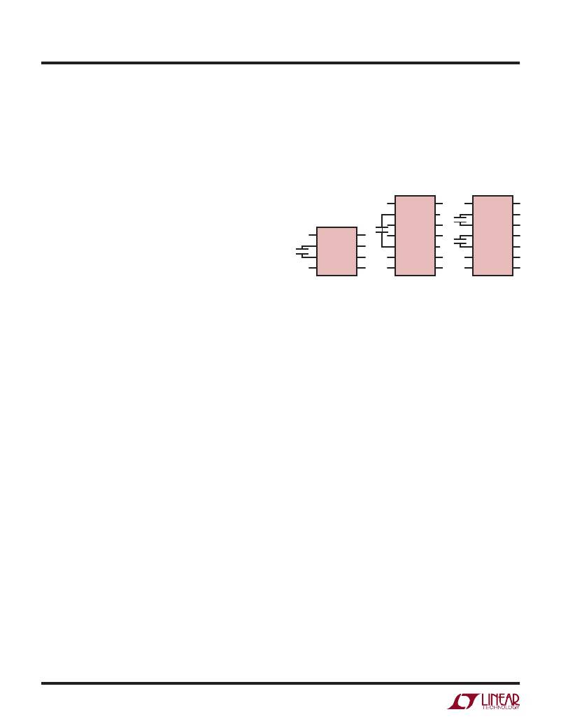
�1� 14� 1� 14�
�2� +� 13� 2� 13�
�3� 12� C1� 3� 12�
�1� 8� C1� 4� 11� 4� 11�
�2� 7� 5� 10� C2� 5� 10�
�–�
�4� 5� 7� 8� 7� 8�
�Doubler� Mode�
�a.)� LTC1261CS8�
�DOUBLER� MODE�
�b.)� LTC1261CS�
�DOUBLER� MODE�
�c.)� LTC1261CS�
�TRIPLER� MODE�
�Doubler� mode� allows� the� LTC1261� to� generate� negative�
�output� voltage� magnitudes� up� to� that� of� the� supply� volt-�
�age,� creating� a� voltage� between� V� CC� and� OUT� of� up� to� two�
�times� V� S� .� In� doubler� mode� the� LT1261� uses� a� single� flying�
�capacitor� to� invert� the� input� supply� voltage,� and� the� output�
�voltage� is� stored� on� the� output� bypass� capacitor� between�
�switch� cycles.� The� LTC1261CS8� is� always� configured� in�
�doubler� mode� and� has� only� one� pair� of� flying� capacitor�
�pins� (Figure� 1a).� The� LTC1261CS� can� be� configured� in�
�doubler� mode� by� connecting� a� single� flying� capacitor�
�between� the� C1� +� and� C2� –� pins.� C1� –� and� C2� +� should� be�
�left� floating� (Figure� 1b).�
�Tripler� Mode�
�The� LTC1261CS� can� be� used� in� a� tripler� mode� which� can�
�generate� negative� output� voltages� up� to� twice� the� supply�
�voltage.� The� total� voltage� between� the� V� CC� and� OUT� pins�
�can� be� up� to� three� times� V� S� .� For� example,� tripler� mode�
�can� be� used� to� generate� –� 5V� from� a� single� positive� 3.3V�
�supply.� Tripler� mode� requires� two� external� flying� capacitors.�
�The� first� connects� between� C1� +� and� C1� –� and� the� second�
�between� C2� +� and� C2� –� (Figure� 1c).� Because� of� the� relatively�
�high� voltages� that� can� be� generated� in� this� mode,� care� must�
�be� taken� to� ensure� that� the� total� input-to-output� voltage�
�never� exceeds� 12V� or� the� LTC1261� may� be� damaged.� In�
�most� applications� the� output� voltage� will� be� kept� in� check�
�LTC1261� ?� F01�
�Figure� 1.� Flying� Capacitor� Connections�
�THEORY� OF� OPERATION�
�A� block� diagram� of� the� LTC1261� is� shown� in� Figure� 2.� The�
�heart� of� the� LTC1261� is� the� charge� pump� core� shown� in� the�
�dashed� box.� It� generates� a� negative� output� voltage� by� first�
�charging� the� flying� capacitors� between� V� CC� and� ground.�
�It� then� stacks� the� flying� capacitors� on� top� of� each� other�
�and� connects� the� top� of� the� stack� to� ground� forcing� the�
�bottom� of� the� stack� to� a� negative� voltage.� The� charge� on�
�the� flying� capacitors� is� transferred� to� the� output� bypass�
�capacitor,� leaving� it� charged� to� the� negative� output� voltage.�
�This� process� is� driven� by� the� internal� clock.�
�Figure� 2� shows� the� charge� pump� configured� in� tripler� mode.�
�With� the� clock� low,� C1� and� C2� are� charged� to� V� CC� by� S1,�
�S3,� S5� and� S7.� At� the� next� rising� clock� edge,� S1,� S3,� S5�
�and� S7� open� and� S2,� S4� and� S6� close,� stacking� C1� and�
�C2� on� top� of� each� other.� S2� connects� C1� +� to� ground,� S4�
�connects� C1� –� to� C2� +� and� C2� –� is� connected� to� the� output�
�by� S6.� The� charge� in� C1� and� C2� is� transferred� to� C� OUT� ,�
�setting� it� to� a� negative� voltage.� Doubler� mode� works� the�
�same� way� except� that� the� single� flying� capacitor� (C1)� is�
�connected� between� C1� +� and� C2� –� .� S3,� S4� and� S5� don’t� do�
�anything� useful� in� doubler� mode.� C1� is� charged� initially�
�by� S1� and� S7� and� connected� to� the� output� by� S2� and� S6.�
�1261fb�
�6�
�For� more� information� www.linear.com/LTC1261�
�相关PDF资料 |
PDF描述 |
|---|---|
| LTC1502CS8-3.3#TR | IC REG SWITCHED CAP 3.3V 8SOIC |
| GEC60DRTH-S13 | CONN EDGECARD 120POS .100 EXTEND |
| GEC60DREN-S13 | CONN EDGECARD 120POS .100 EXTEND |
| GEC60DREH-S13 | CONN EDGECARD 120POS .100 EXTEND |
| LTC3240EDC-3.3#TRPBF | IC REG MULTI CONFIG 3.3V 6DFN |
相关代理商/技术参数 |
参数描述 |
|---|---|
| LTC1261IS8 | 功能描述:IC REG SWITCHD CAP INV ADJ 8SOIC RoHS:否 类别:集成电路 (IC) >> PMIC - 稳压器 - DC DC 开关稳压器 系列:- 标准包装:2,500 系列:- 类型:升压(升压) 输出类型:可调式 输出数:1 输出电压:1.24 V ~ 30 V 输入电压:1.5 V ~ 12 V PWM 型:电流模式,混合 频率 - 开关:600kHz 电流 - 输出:500mA 同步整流器:无 工作温度:-40°C ~ 85°C 安装类型:表面贴装 封装/外壳:8-SOIC(0.154",3.90mm 宽) 包装:带卷 (TR) 供应商设备封装:8-SOIC |
| LTC1261IS8#PBF | 功能描述:IC REG SWITCHD CAP INV ADJ 8SOIC RoHS:是 类别:集成电路 (IC) >> PMIC - 稳压器 - DC DC 开关稳压器 系列:- 标准包装:2,500 系列:- 类型:升压(升压) 输出类型:可调式 输出数:1 输出电压:1.24 V ~ 30 V 输入电压:1.5 V ~ 12 V PWM 型:电流模式,混合 频率 - 开关:600kHz 电流 - 输出:500mA 同步整流器:无 工作温度:-40°C ~ 85°C 安装类型:表面贴装 封装/外壳:8-SOIC(0.154",3.90mm 宽) 包装:带卷 (TR) 供应商设备封装:8-SOIC |
| LTC1261IS8#TR | 功能描述:IC REG SWITCHD CAP INV ADJ 8SOIC RoHS:否 类别:集成电路 (IC) >> PMIC - 稳压器 - DC DC 开关稳压器 系列:- 标准包装:2,500 系列:- 类型:升压(升压) 输出类型:可调式 输出数:1 输出电压:1.24 V ~ 30 V 输入电压:1.5 V ~ 12 V PWM 型:电流模式,混合 频率 - 开关:600kHz 电流 - 输出:500mA 同步整流器:无 工作温度:-40°C ~ 85°C 安装类型:表面贴装 封装/外壳:8-SOIC(0.154",3.90mm 宽) 包装:带卷 (TR) 供应商设备封装:8-SOIC |
| LTC1261IS8#TRPBF | 功能描述:IC REG SWITCHD CAP INV ADJ 8SOIC RoHS:是 类别:集成电路 (IC) >> PMIC - 稳压器 - DC DC 开关稳压器 系列:- 标准包装:2,500 系列:- 类型:升压(升压) 输出类型:可调式 输出数:1 输出电压:1.24 V ~ 30 V 输入电压:1.5 V ~ 12 V PWM 型:电流模式,混合 频率 - 开关:600kHz 电流 - 输出:500mA 同步整流器:无 工作温度:-40°C ~ 85°C 安装类型:表面贴装 封装/外壳:8-SOIC(0.154",3.90mm 宽) 包装:带卷 (TR) 供应商设备封装:8-SOIC |
| LTC1261LCMS8 | 功能描述:IC REG SWITCHD CAP INV ADJ 8MSOP RoHS:否 类别:集成电路 (IC) >> PMIC - 稳压器 - DC DC 开关稳压器 系列:- 标准包装:2,500 系列:- 类型:升压(升压) 输出类型:可调式 输出数:1 输出电压:1.24 V ~ 30 V 输入电压:1.5 V ~ 12 V PWM 型:电流模式,混合 频率 - 开关:600kHz 电流 - 输出:500mA 同步整流器:无 工作温度:-40°C ~ 85°C 安装类型:表面贴装 封装/外壳:8-SOIC(0.154",3.90mm 宽) 包装:带卷 (TR) 供应商设备封装:8-SOIC |
发布紧急采购,3分钟左右您将得到回复。