- 您现在的位置:买卖IC网 > PDF目录14178 > LTC1261CS8-4.5#TRPBF (Linear Technology)IC REG SWITCHED CAP INV 8SOIC PDF资料下载
参数资料
| 型号: | LTC1261CS8-4.5#TRPBF |
| 厂商: | Linear Technology |
| 文件页数: | 8/18页 |
| 文件大小: | 0K |
| 描述: | IC REG SWITCHED CAP INV 8SOIC |
| 标准包装: | 2,500 |
| 类型: | 切换式电容器(充电泵),反相 |
| 输出类型: | 固定 |
| 输出数: | 1 |
| 输出电压: | -4.5V |
| 输入电压: | 3 V ~ 8 V |
| 频率 - 开关: | 550kHz |
| 电流 - 输出: | 15mA |
| 同步整流器: | 无 |
| 工作温度: | 0°C ~ 70°C |
| 安装类型: | 表面贴装 |
| 封装/外壳: | 8-SOIC(0.154",3.90mm 宽) |
| 包装: | 带卷 (TR) |
| 供应商设备封装: | 8-SOIC |
�� �
�
�LTC1261�
�APPLICATIONS� INFORMATION�
�?� ?� =� 15mA� ?� ?� ?� 3.3μF� ?� ?� =� 8.2mV�
�I� LOAD� ?� ?�
�OUTPUTRIPPLE�
�Output� ripple� in� the� LTC1261� comes� from� two� sources;�
�voltage� droop� at� the� output� capacitor� between� clocks� and�
�frequency� response� of� the� regulation� loop.� Voltage� droop�
�is� easy� to� calculate.� With� a� typical� clock� frequency� of�
�550kHz,� the� charge� on� the� output� capacitor� is� refreshed�
�once� every� 1.8μs.� With� a� 15mA� load� and� a� 3.3μF� output�
�capacitor,� the� output� will� droop� by:�
�?� ?� t� ?� ?� 1.8μs� ?�
�?� C� OUT�
�To� prevent� this� from� happening,� an� external� capacitor�
�can� be� connected� from� ADJ� (or� COMP� for� fixed� output�
�parts)� to� ground� to� compensate� for� external� parasitics� and�
�increase� the� regulation� loop� bandwidth� (Figure� 3).� This�
�sounds� coutnterintuitive� until� we� remember� that� the� internal�
�reference� is� generated� with� respect� to� OUT,� not� ground.�
�TO� CHARGE�
�PUMP�
�RESISTORS� ARE�
�INTERNAL� FOR�
�FIXED� OUTPUT� PARTS�
�+�
�–�
�This� can� be� a� significant� ripple� component� when� the� output�
�is� heavily� loaded,� especially� if� the� output� capacitor� is� small.�
�If� absolute� minimum� output� ripple� is� required,� a� 10μF� or�
�greater� output� capacitor� should� be� used.�
�REF�
�COMP� 1�
�1.24V�
�R1�
�R2�
�C� C�
�100pF�
�ADJ/COMP�
�V� OUT�
�Regulation� loop� frequency� response� is� the� other� major�
�contributor� to� output� ripple.� The� LTC1261� regulates� the�
�output� voltage� by� limiting� the� amount� of� charge� transferred�
�to� the� output� capacitor� on� a� cycle-by-cycle� basis.� The�
�output� voltage� is� sensed� at� the� ADJ� pin� (COMP� for� fixed�
�output� versions)� through� an� internal� or� external� resistor�
�divider� from� the� OUT� pin� to� ground.� As� the� flying� capaci-�
�tors� are� first� connected� to� the� output,� the� output� voltage�
�begins� to� change� quite� rapidly.� As� soon� as� it� exceeds� the�
�set� point� COMP1� trips,� switching� the� state� of� the� charge�
�pump� and� stopping� the� charge� transfer.� Because� the� RC�
�time� constant� of� the� capacitors� and� the� switches� is� quite�
�short,� the� ADJ� pin� must� have� a� wide� AC� bandwidth� to� be�
�able� to� respond� to� the� output� in� time.� External� parasitic�
�capacitance� at� the� ADJ� pin� can� reduce� the� bandwidth� to�
�the� point� where� the� comparator� cannot� respond� by� the�
�time� the� clock� pulse� finishes.� When� this� happens� the�
�comparator� will� allow� a� few� complete� pulses� through,� then�
�overcorrect� and� disable� the� charge� pump� until� the� output�
�drops� below� the� set� point.� Under� these� conditions� the�
�output� will� remain� in� regulation� but� the� output� ripple� will�
�increase� as� the� comparator� “hunts”� for� the� correct� value.�
�LTC1261� ?� F03�
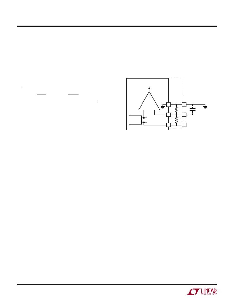
�Figure� 3.� Regulator� Loop� Compensation�
�The� feedback� loop� actually� sees� ground� as� its� “output,”� thus�
�the� compensation� capacitor� should� be� connected� across�
�the� “top”� of� the� resistor� divider,� from� ADJ� (or� COMP)� to�
�ground.� By� the� same� token,� avoid� adding� capacitance�
�between� ADJ� (or� COMP)� and� V� OUT� .� This� will� slow� down�
�the� feedback� loop� and� increase� output� ripple.� A� 100pF�
�capacitor� from� ADJ� or� COMP� to� ground� will� compensate�
�the� loop� properly� under� most� conditions.�
�OUTPUT� FILTERING�
�If� extremely� low� output� ripple� (<� 5mV)� is� required,� addi-�
�tional� output� filtering� is� required.� Because� the� LTC1261�
�uses� a� high� 550kHz� switching� frequency,� fairly� low� value�
�RC� or� LC� networks� can� be� used� at� the� output� to� effectively�
�filter� the� output� ripple.� A� 10Ω� series� output� resistor� and�
�a� 3.3μF� capacitor� will� cut� output� ripple� to� below� 3mV�
�(Figure?4).� Further� reductions� can� be� obtained� with� larger�
�filter� capacitors� or� by� using� an� LC� output� filter.�
�1261fb�
�8�
�For� more� information� www.linear.com/LTC1261�
�相关PDF资料 |
PDF描述 |
|---|---|
| LTC1261CS8-4.5#TR | IC REG SWITCHED CAP INV 8SOIC |
| LTC1502CS8-3.3#TR | IC REG SWITCHED CAP 3.3V 8SOIC |
| GEC60DRTH-S13 | CONN EDGECARD 120POS .100 EXTEND |
| GEC60DREN-S13 | CONN EDGECARD 120POS .100 EXTEND |
| GEC60DREH-S13 | CONN EDGECARD 120POS .100 EXTEND |
相关代理商/技术参数 |
参数描述 |
|---|---|
| LTC1261IS8 | 功能描述:IC REG SWITCHD CAP INV ADJ 8SOIC RoHS:否 类别:集成电路 (IC) >> PMIC - 稳压器 - DC DC 开关稳压器 系列:- 标准包装:2,500 系列:- 类型:升压(升压) 输出类型:可调式 输出数:1 输出电压:1.24 V ~ 30 V 输入电压:1.5 V ~ 12 V PWM 型:电流模式,混合 频率 - 开关:600kHz 电流 - 输出:500mA 同步整流器:无 工作温度:-40°C ~ 85°C 安装类型:表面贴装 封装/外壳:8-SOIC(0.154",3.90mm 宽) 包装:带卷 (TR) 供应商设备封装:8-SOIC |
| LTC1261IS8#PBF | 功能描述:IC REG SWITCHD CAP INV ADJ 8SOIC RoHS:是 类别:集成电路 (IC) >> PMIC - 稳压器 - DC DC 开关稳压器 系列:- 标准包装:2,500 系列:- 类型:升压(升压) 输出类型:可调式 输出数:1 输出电压:1.24 V ~ 30 V 输入电压:1.5 V ~ 12 V PWM 型:电流模式,混合 频率 - 开关:600kHz 电流 - 输出:500mA 同步整流器:无 工作温度:-40°C ~ 85°C 安装类型:表面贴装 封装/外壳:8-SOIC(0.154",3.90mm 宽) 包装:带卷 (TR) 供应商设备封装:8-SOIC |
| LTC1261IS8#TR | 功能描述:IC REG SWITCHD CAP INV ADJ 8SOIC RoHS:否 类别:集成电路 (IC) >> PMIC - 稳压器 - DC DC 开关稳压器 系列:- 标准包装:2,500 系列:- 类型:升压(升压) 输出类型:可调式 输出数:1 输出电压:1.24 V ~ 30 V 输入电压:1.5 V ~ 12 V PWM 型:电流模式,混合 频率 - 开关:600kHz 电流 - 输出:500mA 同步整流器:无 工作温度:-40°C ~ 85°C 安装类型:表面贴装 封装/外壳:8-SOIC(0.154",3.90mm 宽) 包装:带卷 (TR) 供应商设备封装:8-SOIC |
| LTC1261IS8#TRPBF | 功能描述:IC REG SWITCHD CAP INV ADJ 8SOIC RoHS:是 类别:集成电路 (IC) >> PMIC - 稳压器 - DC DC 开关稳压器 系列:- 标准包装:2,500 系列:- 类型:升压(升压) 输出类型:可调式 输出数:1 输出电压:1.24 V ~ 30 V 输入电压:1.5 V ~ 12 V PWM 型:电流模式,混合 频率 - 开关:600kHz 电流 - 输出:500mA 同步整流器:无 工作温度:-40°C ~ 85°C 安装类型:表面贴装 封装/外壳:8-SOIC(0.154",3.90mm 宽) 包装:带卷 (TR) 供应商设备封装:8-SOIC |
| LTC1261LCMS8 | 功能描述:IC REG SWITCHD CAP INV ADJ 8MSOP RoHS:否 类别:集成电路 (IC) >> PMIC - 稳压器 - DC DC 开关稳压器 系列:- 标准包装:2,500 系列:- 类型:升压(升压) 输出类型:可调式 输出数:1 输出电压:1.24 V ~ 30 V 输入电压:1.5 V ~ 12 V PWM 型:电流模式,混合 频率 - 开关:600kHz 电流 - 输出:500mA 同步整流器:无 工作温度:-40°C ~ 85°C 安装类型:表面贴装 封装/外壳:8-SOIC(0.154",3.90mm 宽) 包装:带卷 (TR) 供应商设备封装:8-SOIC |
发布紧急采购,3分钟左右您将得到回复。