- 您现在的位置:买卖IC网 > PDF目录44988 > LTC1266IS-5 (LINEAR TECHNOLOGY CORP) SWITCHING CONTROLLER, 400 kHz SWITCHING FREQ-MAX, PDSO16 PDF资料下载
参数资料
| 型号: | LTC1266IS-5 |
| 厂商: | LINEAR TECHNOLOGY CORP |
| 元件分类: | 稳压器 |
| 英文描述: | SWITCHING CONTROLLER, 400 kHz SWITCHING FREQ-MAX, PDSO16 |
| 封装: | 0.150 INCH, PLASTIC, SO-16 |
| 文件页数: | 18/20页 |
| 文件大小: | 240K |
| 代理商: | LTC1266IS-5 |
7
LTC1266
LTC1266-3.3/LTC1266-5
Pin 10 Connection Shown for LTC1266-3.3 and LTC1266-5; Changes Create LTC1266
+
–
16
4
1
3
15 PGND
BDRIVE
TDRIVE
PINV
BINH
2
PWR VIN
R
S
Q
–
+
C
VTRIP
7
13k
ITH
PINV
1.265V
11
5
REFERENCE
–
+
SHDN
VIN
VOS
–
+
V
G
9
SENSE+
10
ADJUSTABLE
VERSION
VFB
100k
5pF
–
+
VTH1
T
–
+
VTH2
S
SLEEP
12
SIGNAL
GROUND
6
CT
OFF-TIME
CONTROL
MAX
ON-TIME
CONTROL
VIN
SENSE–
VFB
SENSE–
8
1266 FD
ENABLE
LBOUT
LBIN
VIN
14
–
+
LB
13
1.25V
REFERENCE
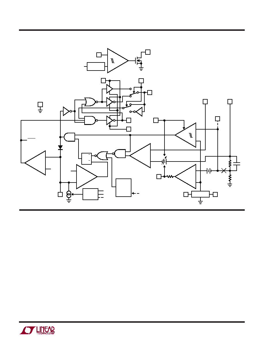
The LTC1266 series uses a current mode, constant off-
time architecture to synchronously switch an external pair
of power MOSFETs. Operating frequency is set by an
external capacitor at the timing capacitor Pin 6.
The output voltage is sensed by an internal voltage divider
connected to SENSE –, Pin 8, (LTC1266-3.3 and LTC1266-
5) or external divider returned to VFB, Pin 10, (LTC1266).
A voltage comparator V, and a gain block G, compare the
divided output voltage with a reference voltage of 1.265V.
To optimize efficiency, the LTC1266 automatically switches
between two modes of operation, burst and continuous.
The voltage comparator is the primary control element
when the device is in Burst Modeoperation, while the gain
block controls the output voltage in continuous mode.
During the switch ON cycle in continuous mode, current
comparator C monitors the voltage between Pins 8 and 9
connected across an external shunt in series with the
inductor. When the voltage across the shunt reaches its
threshold value, the topside driver output is switched to
turn off the topside MOFSET (Power VIN for P-channel or
ground for N-channel). The timing capacitor connected to
Pin 6 is now allowed to discharge at a rate determined by
the off-time controller. The discharge current is made
proportional to the output voltage (measured by Pin 8) to
model the inductor current, which decays at a rate which
is also proportional to the output voltage. While the timing
capacitor is discharging, the bottom-side drive output is
switched to power VIN to turn on the bottom-side
N-channel MOSFET.
FU CTIO AL DIAGRA
U
W
OPERATIO
U
相关PDF资料 |
PDF描述 |
|---|---|
| LTC1474CS8-3.3#TR | 0.75 A SWITCHING REGULATOR, PDSO8 |
| LTC1474IS8-5#TR | 0.75 A SWITCHING REGULATOR, PDSO8 |
| LTC1530CS8-1.9#TR | SWITCHING CONTROLLER, 350 kHz SWITCHING FREQ-MAX, PDSO8 |
| LTC1530IS8-2.5#PBF | SWITCHING CONTROLLER, 350 kHz SWITCHING FREQ-MAX, PDSO8 |
| LTC1530CS8-2.8#TR | SWITCHING CONTROLLER, 350 kHz SWITCHING FREQ-MAX, PDSO8 |
相关代理商/技术参数 |
参数描述 |
|---|---|
| LTC1266IS-5#PBF | 功能描述:IC REG CTRLR BST PWM CM 16-SOIC RoHS:是 类别:集成电路 (IC) >> PMIC - 稳压器 - DC DC 切换控制器 系列:- 标准包装:4,000 系列:- PWM 型:电压模式 输出数:1 频率 - 最大:1.5MHz 占空比:66.7% 电源电压:4.75 V ~ 5.25 V 降压:是 升压:无 回扫:无 反相:无 倍增器:无 除法器:无 Cuk:无 隔离:无 工作温度:-40°C ~ 85°C 封装/外壳:40-VFQFN 裸露焊盘 包装:带卷 (TR) |
| LTC1266IS-5#TR | 功能描述:IC REG CTRLR BST PWM CM 16-SOIC RoHS:否 类别:集成电路 (IC) >> PMIC - 稳压器 - DC DC 切换控制器 系列:- 标准包装:2,500 系列:- PWM 型:电流模式 输出数:1 频率 - 最大:500kHz 占空比:96% 电源电压:4 V ~ 36 V 降压:无 升压:是 回扫:无 反相:无 倍增器:无 除法器:无 Cuk:无 隔离:无 工作温度:-40°C ~ 125°C 封装/外壳:24-WQFN 裸露焊盘 包装:带卷 (TR) |
| LTC1266IS-5#TRPBF | 功能描述:IC REG CTRLR BST PWM CM 16-SOIC RoHS:是 类别:集成电路 (IC) >> PMIC - 稳压器 - DC DC 切换控制器 系列:- 标准包装:4,000 系列:- PWM 型:电压模式 输出数:1 频率 - 最大:1.5MHz 占空比:66.7% 电源电压:4.75 V ~ 5.25 V 降压:是 升压:无 回扫:无 反相:无 倍增器:无 除法器:无 Cuk:无 隔离:无 工作温度:-40°C ~ 85°C 封装/外壳:40-VFQFN 裸露焊盘 包装:带卷 (TR) |
| LTC1267CG-ADJ | 制造商:Linear Technology 功能描述:Dual High Efficiency Synchronous Step-Down Switching Regulators |
| LTC1272-3ACN | 功能描述:IC A/D CONV 12BIT SAMPLING 24DIP RoHS:否 类别:集成电路 (IC) >> 数据采集 - 模数转换器 系列:- 标准包装:1,000 系列:- 位数:12 采样率(每秒):300k 数据接口:并联 转换器数目:1 功率耗散(最大):75mW 电压电源:单电源 工作温度:0°C ~ 70°C 安装类型:表面贴装 封装/外壳:24-SOIC(0.295",7.50mm 宽) 供应商设备封装:24-SOIC 包装:带卷 (TR) 输入数目和类型:1 个单端,单极;1 个单端,双极 |
发布紧急采购,3分钟左右您将得到回复。