- 您现在的位置:买卖IC网 > PDF目录44988 > LTC1266IS#TR-3.3 (LINEAR TECHNOLOGY CORP) SWITCHING CONTROLLER, 400 kHz SWITCHING FREQ-MAX, PDSO16 PDF资料下载
参数资料
| 型号: | LTC1266IS#TR-3.3 |
| 厂商: | LINEAR TECHNOLOGY CORP |
| 元件分类: | 稳压器 |
| 英文描述: | SWITCHING CONTROLLER, 400 kHz SWITCHING FREQ-MAX, PDSO16 |
| 封装: | 0.150 INCH, PLASTIC, SO-16 |
| 文件页数: | 17/20页 |
| 文件大小: | 245K |
| 代理商: | LTC1266IS#TR-3.3 |
6
LTC1266
LTC1266-3.3/LTC1266-5
TDRIVE (Pin 1): High Current Drive for Topside MOSFET.
This MOSFET can be either P-channel or N-channel, user
selectable by Pin 3. Voltage swing at this pin is from PWR
VIN to ground.
PWR VIN (Pin 2): Power Suppy for Drive Signals. Must be
closely decoupled to power ground (Pin 15).
PINV (Pin 3): Phase Invert. Sets the phase of the topside
driver to drive either a P-channel or an N-channel MOSFET
as follows:
P-channel: Pin 3 = 0V
N-channel: Pin 3 = PWR VIN
BINH (Pin 4): Burst Mode Operation Inhibit. A CMOS logic
high on this pin will disable the Burst Mode operation
feature forcing continuous operation down to zero load.
VIN (Pin 5): Main Supply Pin.
CT (Pin 6): External Capacitor. CT from Pin 4 to ground sets
the operating frequency. The actual frequency is also
dependent on the input voltage.
ITH (Pin 7): Gain Amplifier Decoupling Point. The current
comparator threshold increases with the Pin 7 voltage.
SENSE – (Pin 8): Connects to internal resistive divider
which sets the output voltage in LTC1266-3.3 and
LTC1266-5 versions. Pin 8 is also the (–) input for the
current comparator.
SENSE + (Pin 9): The (+) Input to the Current Comparator.
A built-in offset between Pins 8 and 9 in conjunction with
RSENSE sets the current trip threshold.
VFB (Pin 10): For the LTC1266 adjustable version, Pin 10
serves as the feedback pin from an external resistive
divider used to set the output voltage. On LTC1266-3.3
and LTC1266-5 versions this pin is not used.
SHDN (Pin 11): When grounded, the LTC1266 series
operates normally. Pulling Pin 11 high holds both
MOSFETs off and puts the LTC1266 in micropower shut-
down mode. Requires CMOS logic signal with tr, tf < 1s.
Should not be left floating.
SGND (Pin 12): Small-Signal Ground. Must be routed
separately from other grounds to the (–) terminal of COUT.
LBIN (Pin 13): Input to the Low-Battery Comparator. This
input is compared to an internal 1.25V reference.
LBOUT (Pin 14): Open Drain Output of the Low-Battery
Comparator. This pin will sink current when Pin 13 is
below 1.25V.
PGND (Pin 15): Driver Power Ground. Connects to source
of N-channel MOSFET and the (–) terminal of CIN.
BDRIVE (Pin 16): High Current Drive for Bottom
N-Channel MOSFET. Voltage swing at Pin 16 is from
ground to PWR VIN.
UU
U
PI FU CTIO S
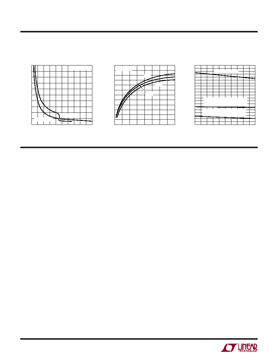
OUTPUT VOLTAGE (V)
01
OFF-TIME
(
s)
40
60
5
1266 G10
20
0
2
34
100
80
LTC1266-3.3
LTC1266-5
VSENSE
– = VOUT
(VIN – VOUT) VOLTAGE (V)
0
NORMALIZED
FREQUENCY
2.5
3.0
12
10
8
1266 G11
0.5
1.5
2.0
1.0
0
2
4
6
14
16
VOUT = 3.3V
0
°C
70
°C
25
°C
TEMPERATURE (
°C)
0
SENSE
VOLTAGE
(mV)
100
150
200
80
1266 G12
50
0
–50
20
40
60
100
MAX THRESHOLD
MIN THRESHOLD (Burst Mode
OPERATION INHIBIT)
MIN THRESHOLD (Burst Mode
OPERATION ENABLED)
Off-Time vs Output Voltage
Operating Frequency
vs (VIN – VOUT) Voltage
Current Sense Threshold Voltage
TYPICAL PERFOR A CE CHARACTERISTICS
UW
相关PDF资料 |
PDF描述 |
|---|---|
| LTC1266IS#TR-5 | SWITCHING CONTROLLER, 400 kHz SWITCHING FREQ-MAX, PDSO16 |
| LTC1266IS-5 | SWITCHING CONTROLLER, 400 kHz SWITCHING FREQ-MAX, PDSO16 |
| LTC1474CS8-3.3#TR | 0.75 A SWITCHING REGULATOR, PDSO8 |
| LTC1474IS8-5#TR | 0.75 A SWITCHING REGULATOR, PDSO8 |
| LTC1530CS8-1.9#TR | SWITCHING CONTROLLER, 350 kHz SWITCHING FREQ-MAX, PDSO8 |
相关代理商/技术参数 |
参数描述 |
|---|---|
| LTC1267CG-ADJ | 制造商:Linear Technology 功能描述:Dual High Efficiency Synchronous Step-Down Switching Regulators |
| LTC1272-3ACN | 功能描述:IC A/D CONV 12BIT SAMPLING 24DIP RoHS:否 类别:集成电路 (IC) >> 数据采集 - 模数转换器 系列:- 标准包装:1,000 系列:- 位数:12 采样率(每秒):300k 数据接口:并联 转换器数目:1 功率耗散(最大):75mW 电压电源:单电源 工作温度:0°C ~ 70°C 安装类型:表面贴装 封装/外壳:24-SOIC(0.295",7.50mm 宽) 供应商设备封装:24-SOIC 包装:带卷 (TR) 输入数目和类型:1 个单端,单极;1 个单端,双极 |
| LTC1272-3ACN#PBF | 功能描述:IC A/D CONV 12BIT SAMPLING 24DIP RoHS:是 类别:集成电路 (IC) >> 数据采集 - 模数转换器 系列:- 标准包装:1,000 系列:- 位数:12 采样率(每秒):300k 数据接口:并联 转换器数目:1 功率耗散(最大):75mW 电压电源:单电源 工作温度:0°C ~ 70°C 安装类型:表面贴装 封装/外壳:24-SOIC(0.295",7.50mm 宽) 供应商设备封装:24-SOIC 包装:带卷 (TR) 输入数目和类型:1 个单端,单极;1 个单端,双极 |
| LTC1272-3ACSW | 功能描述:IC A/D CONV 12BIT SAMPLNG 24SOIC RoHS:否 类别:集成电路 (IC) >> 数据采集 - 模数转换器 系列:- 其它有关文件:TSA1204 View All Specifications 标准包装:1 系列:- 位数:12 采样率(每秒):20M 数据接口:并联 转换器数目:2 功率耗散(最大):155mW 电压电源:模拟和数字 工作温度:-40°C ~ 85°C 安装类型:表面贴装 封装/外壳:48-TQFP 供应商设备封装:48-TQFP(7x7) 包装:Digi-Reel® 输入数目和类型:4 个单端,单极;2 个差分,单极 产品目录页面:1156 (CN2011-ZH PDF) 其它名称:497-5435-6 |
| LTC1272-3ACSW#PBF | 功能描述:IC A/D CONV 12BIT SAMPLNG 24SOIC RoHS:是 类别:集成电路 (IC) >> 数据采集 - 模数转换器 系列:- 其它有关文件:TSA1204 View All Specifications 标准包装:1 系列:- 位数:12 采样率(每秒):20M 数据接口:并联 转换器数目:2 功率耗散(最大):155mW 电压电源:模拟和数字 工作温度:-40°C ~ 85°C 安装类型:表面贴装 封装/外壳:48-TQFP 供应商设备封装:48-TQFP(7x7) 包装:Digi-Reel® 输入数目和类型:4 个单端,单极;2 个差分,单极 产品目录页面:1156 (CN2011-ZH PDF) 其它名称:497-5435-6 |
发布紧急采购,3分钟左右您将得到回复。