- 您现在的位置:买卖IC网 > PDF目录10225 > LTC1275BCN#PBF (Linear Technology)IC A/D CONV 12BIT SAMPLING 24DIP PDF资料下载
参数资料
| 型号: | LTC1275BCN#PBF |
| 厂商: | Linear Technology |
| 文件页数: | 9/24页 |
| 文件大小: | 0K |
| 描述: | IC A/D CONV 12BIT SAMPLING 24DIP |
| 标准包装: | 15 |
| 位数: | 12 |
| 采样率(每秒): | 300k |
| 数据接口: | 并联 |
| 转换器数目: | 1 |
| 功率耗散(最大): | 75mW |
| 电压电源: | 双 ± |
| 工作温度: | 0°C ~ 70°C |
| 安装类型: | 通孔 |
| 封装/外壳: | 24-DIP(0.300",7.62mm) |
| 供应商设备封装: | 24-PDIP |
| 包装: | 管件 |
| 输入数目和类型: | 1 个单端,单极;1 个单端,双极 |
17
LTC1273
LTC1275/LTC1276
127356fa
U
S
A
O
PPLICATI
WU
U
I FOR ATIO
OLD DATA
DB7-DB0
NEW DATA
DB7-DB0
TRACK
HOLD
DATA
BUSY
RD
CS
RD
LTC1273/75/76 F14
t8
t1
t2
t 3
t CONV
t11
t9
t8
t9
t5
t1
t4
t5
t10
t6
t7
t3
t7
t12
HBEN
NEW DATA
DB11-DB8
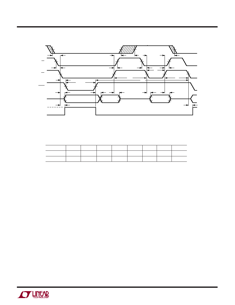
Figure 14. Slow Memory Mode, Two Byte Read Timing Diagram
Table 3. Slow Memory Mode, Two Byte Read Data Bus Status
Data Outputs
D7
D6
D5
D4
D3/11
D2/10
D1/9
D0/8
First Read
DB7
DB6
DB5
DB4
DB3
DB2
DB1
DB0
Second Read
Low
DB11
DB10
DB9
DB8
that the 4MSBs appear on data output D11...D8 during
both READ operations.
ROM Mode, Parallel Read (HBEN = LOW)
The ROM Mode avoids placing a microprocessor into a
WAIT state. A conversion is started with a READ opera-
tion, and the 12 bits of data from the previous conversion
are available on data outputs D11...D0/8 (see Figure 15
and Table 4). This data may be disregarded if not re-
quired. A second READ operation reads the new data
(DB11...DB0) and starts another conversion. A delay at
least as long as the ADC’s conversion time plus the 600ns
minimum delay between conversions must be allowed
between READ operations.
ROM Mode, Two Byte Read
As previously mentioned for a two byte read, only data
outputs D7...D0/8 are used. Conversion is started in the
normal way with a READ operation and the data output
status is the same as the ROM mode, Parallel Read (see
Figure 16 timing diagram and Table 5 data bus status).
Two more READ operations are required to access the new
conversion result. A delay equal at the ADCs’ conversion
time must be allowed between conversion start and the
third data READ operation. The second READ operation
with HBEN high disables conversion start and places the
high byte (4MSBs) on data outputs D3/11...D0/8. A third
read operation accesses the low data byte (DB7...DB0)
and starts another conversion. The 4MSBs appear on data
outputs D11...D8 during all three read operations.
MICROPROCESSOR INTERFACING
The LTC1273/LTC1275/LTC1276 allow easy interfac-
ing to digital signal processors as well as modern high
speed, 8-bit or 16-bit microprocessors. Here are sev-
eral examples.
相关PDF资料 |
PDF描述 |
|---|---|
| SP3220ECA-L/TR | IC DVR/RCVR RS232 ESD 16SSOP |
| SP3220EBCY-L/TR | IC DVR/RCVR RS232 ESD 16TSSOP |
| LTC1407AHMSE#TRPBF | IC ADC 14BIT 3MSPS 10-MSOP |
| AD7866ARU | IC ADC 12BIT 2CH DUAL 20-TSSOP |
| SP26LV432CN-L/TR | IC RCVR RS422 QUAD DIFF 16NSOIC |
相关代理商/技术参数 |
参数描述 |
|---|---|
| LTC1275BCSW | 功能描述:IC A/D CONV 12BIT SAMPLNG 24SOIC RoHS:否 类别:集成电路 (IC) >> 数据采集 - 模数转换器 系列:- 标准包装:1,000 系列:- 位数:12 采样率(每秒):300k 数据接口:并联 转换器数目:1 功率耗散(最大):75mW 电压电源:单电源 工作温度:0°C ~ 70°C 安装类型:表面贴装 封装/外壳:24-SOIC(0.295",7.50mm 宽) 供应商设备封装:24-SOIC 包装:带卷 (TR) 输入数目和类型:1 个单端,单极;1 个单端,双极 |
| LTC1275BCSW#PBF | 功能描述:IC A/D CONV 12BIT SAMPLNG 24SOIC RoHS:是 类别:集成电路 (IC) >> 数据采集 - 模数转换器 系列:- 标准包装:1,000 系列:- 位数:12 采样率(每秒):300k 数据接口:并联 转换器数目:1 功率耗散(最大):75mW 电压电源:单电源 工作温度:0°C ~ 70°C 安装类型:表面贴装 封装/外壳:24-SOIC(0.295",7.50mm 宽) 供应商设备封装:24-SOIC 包装:带卷 (TR) 输入数目和类型:1 个单端,单极;1 个单端,双极 |
| LTC1275BCSW#TR | 功能描述:IC ADC 12BIT SAMPLING REF 24SOIC RoHS:否 类别:集成电路 (IC) >> 数据采集 - 模数转换器 系列:- 标准包装:1,000 系列:- 位数:12 采样率(每秒):300k 数据接口:并联 转换器数目:1 功率耗散(最大):75mW 电压电源:单电源 工作温度:0°C ~ 70°C 安装类型:表面贴装 封装/外壳:24-SOIC(0.295",7.50mm 宽) 供应商设备封装:24-SOIC 包装:带卷 (TR) 输入数目和类型:1 个单端,单极;1 个单端,双极 |
| LTC1275BCSW#TRPBF | 功能描述:IC A/D CONV 12BIT SAMPLNG 24SOIC RoHS:是 类别:集成电路 (IC) >> 数据采集 - 模数转换器 系列:- 标准包装:1,000 系列:- 位数:12 采样率(每秒):300k 数据接口:并联 转换器数目:1 功率耗散(最大):75mW 电压电源:单电源 工作温度:0°C ~ 70°C 安装类型:表面贴装 封装/外壳:24-SOIC(0.295",7.50mm 宽) 供应商设备封装:24-SOIC 包装:带卷 (TR) 输入数目和类型:1 个单端,单极;1 个单端,双极 |
| LTC1276ACN | 功能描述:IC A/D CONV 12BIT SAMPLING 24DIP RoHS:否 类别:集成电路 (IC) >> 数据采集 - 模数转换器 系列:- 标准包装:1,000 系列:- 位数:12 采样率(每秒):300k 数据接口:并联 转换器数目:1 功率耗散(最大):75mW 电压电源:单电源 工作温度:0°C ~ 70°C 安装类型:表面贴装 封装/外壳:24-SOIC(0.295",7.50mm 宽) 供应商设备封装:24-SOIC 包装:带卷 (TR) 输入数目和类型:1 个单端,单极;1 个单端,双极 |
发布紧急采购,3分钟左右您将得到回复。