- 您现在的位置:买卖IC网 > PDF目录10195 > LTC1279ISW#TR (Linear Technology)IC ADC 12BIT SAMPL SHTDWN 24SOIC PDF资料下载
参数资料
| 型号: | LTC1279ISW#TR |
| 厂商: | Linear Technology |
| 文件页数: | 5/16页 |
| 文件大小: | 0K |
| 描述: | IC ADC 12BIT SAMPL SHTDWN 24SOIC |
| 标准包装: | 1,000 |
| 位数: | 12 |
| 采样率(每秒): | 600k |
| 数据接口: | 并联 |
| 转换器数目: | 1 |
| 功率耗散(最大): | 120mW |
| 电压电源: | 双 ± |
| 工作温度: | -40°C ~ 85°C |
| 安装类型: | 表面贴装 |
| 封装/外壳: | 24-SOIC(0.295",7.50mm 宽) |
| 供应商设备封装: | 24-SOIC |
| 包装: | 带卷 (TR) |
| 输入数目和类型: | 1 个单端,单极;1 个单端,双极 |
13
LTC1279
U
S
A
O
PPLICATI
WU
U
I FOR ATIO
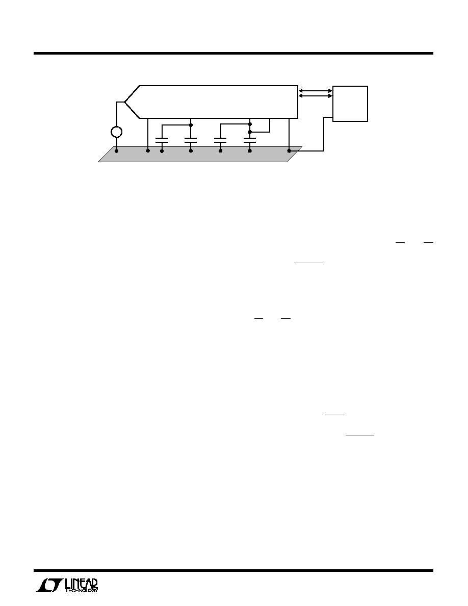
adequate bypassing for the VSS pin. The capacitors must
be located as close to the pins as possible. The traces
connecting the pins and the bypass capacitors must be
kept short and should be made as wide as possible.
Input signal traces to AIN (pin 1) and signal return traces
from AGND (pin 3) should be kept as short as possible to
minimize input noise coupling. In applications where this
is not possible, a shielded cable between the signal source
and ADC is recommended. Also, since any potential differ-
ence in grounds between the signal source and ADC
appears as an error voltage in series with the input signal,
attention should be paid to reducing the ground circuit
impedances as much as possible.
A single point analog ground, separate from the logic
system ground, should be established with an analog
ground plane at pin 3 (AGND) or as close as possible to the
ADC. Pin 12 (DGND) and all other analog grounds should
be connected to this single analog ground point. No other
digital grounds should be connected to this analog ground
point. Low impedance analog and digital power supply
common returns are essential to low noise operation of
the ADC and the foil width for these tracks should be as
wide as possible. In applications where the ADC data
outputs and control signals are connected to a continu-
ously active microprocessor bus, it is possible to get
errors in conversion results. These errors are due to
feedthrough from the microprocessor to the successive
approximation comparator. The problem can be elimi-
nated by forcing the microprocessor into a WAIT state
during conversion or by using three-state buffers to iso-
late the ADC data bus.
DIGITAL INTERFACE
The A/D converter is designed to interface with micropro-
cessors as a memory mapped device. The CS and RD
control inputs are common to all peripheral memory interfac-
ing. A separate CONVST is used to initiate a conversion.
Internal Clock
The A/D converter has an internal clock that eliminates the
need of synchronization between the external clock and
the CS and RD signals found in other ADCs. The internal
clock is factory trimmed to achieve a typical conversion
time of 1.4
s. No external adjustments are required, and
with the typical acquisition time of 160ns, throughput
performance of 600ksps is assured.
Power Shutdown
The LTC1279 provides a power shutdown feature that
saves power when the ADC is in inactive periods. To power
down the ADC, pin 18 (SHDN) needs to be driven low.
When in power shutdown mode, the LTC1279 will not start
a conversion even though the CONVST goes low. All the
power is off except the Internal Reference which is still
active and provides 2.42V output voltage to the other
circuitry. In this mode the ADC draws 8.5mW instead of
60mW (for minimum power, the logic inputs must be
within 600mV of the supply rails). The wake-up time from
the power shutdown to active state is 350ns.
Figure 10. Power Supply Grounding Practice
1279 F10
AIN
AGND
VREF
AVDD
DVDD
DGND
LTC1279
DIGITAL
SYSTEM
0.1
F
+
–
ANALOG GROUND PLANE
GROUND CONNECTION
TO DIGITAL CIRCUITRY
ANALOG
INPUT
CIRCUITRY
3
2
24
17
12
1
0.1
F
10
F
10
F
相关PDF资料 |
PDF描述 |
|---|---|
| VI-BW2-MY | CONVERTER MOD DC/DC 15V 50W |
| PX0745/P | CONN PLUG 7POS W/PINS BLACK |
| VI-BW1-MY | CONVERTER MOD DC/DC 12V 50W |
| D38999/20FB98PC | CONN RCPT 6POS WALL MNT W/PINS |
| D5FBX | CONN RCPT FEMALE 5PIN BLK/SILVER |
相关代理商/技术参数 |
参数描述 |
|---|---|
| LTC1282ACN | 功能描述:IC A/D CONV SAMPLING W/REF 24DIP RoHS:否 类别:集成电路 (IC) >> 数据采集 - 模数转换器 系列:- 标准包装:1,000 系列:- 位数:12 采样率(每秒):300k 数据接口:并联 转换器数目:1 功率耗散(最大):75mW 电压电源:单电源 工作温度:0°C ~ 70°C 安装类型:表面贴装 封装/外壳:24-SOIC(0.295",7.50mm 宽) 供应商设备封装:24-SOIC 包装:带卷 (TR) 输入数目和类型:1 个单端,单极;1 个单端,双极 |
| LTC1282ACN#PBF | 功能描述:IC A/D CONV SAMPLING W/REF 24DIP RoHS:是 类别:集成电路 (IC) >> 数据采集 - 模数转换器 系列:- 产品培训模块:Lead (SnPb) Finish for COTS Obsolescence Mitigation Program 标准包装:2,500 系列:- 位数:12 采样率(每秒):3M 数据接口:- 转换器数目:- 功率耗散(最大):- 电压电源:- 工作温度:- 安装类型:表面贴装 封装/外壳:SOT-23-6 供应商设备封装:SOT-23-6 包装:带卷 (TR) 输入数目和类型:- |
| LTC1282ACSW | 功能描述:IC A/D CONV SAMPLING W/REF24SOIC RoHS:否 类别:集成电路 (IC) >> 数据采集 - 模数转换器 系列:- 标准包装:1,000 系列:- 位数:12 采样率(每秒):300k 数据接口:并联 转换器数目:1 功率耗散(最大):75mW 电压电源:单电源 工作温度:0°C ~ 70°C 安装类型:表面贴装 封装/外壳:24-SOIC(0.295",7.50mm 宽) 供应商设备封装:24-SOIC 包装:带卷 (TR) 输入数目和类型:1 个单端,单极;1 个单端,双极 |
| LTC1282ACSW#PBF | 功能描述:IC A/D CONV SAMPLING W/REF24SOIC RoHS:是 类别:集成电路 (IC) >> 数据采集 - 模数转换器 系列:- 标准包装:1,000 系列:- 位数:12 采样率(每秒):300k 数据接口:并联 转换器数目:1 功率耗散(最大):75mW 电压电源:单电源 工作温度:0°C ~ 70°C 安装类型:表面贴装 封装/外壳:24-SOIC(0.295",7.50mm 宽) 供应商设备封装:24-SOIC 包装:带卷 (TR) 输入数目和类型:1 个单端,单极;1 个单端,双极 |
| LTC1282ACSW#TR | 功能描述:IC ADC 12BIT SAMPLING REF 24SOIC RoHS:否 类别:集成电路 (IC) >> 数据采集 - 模数转换器 系列:- 标准包装:1,000 系列:- 位数:12 采样率(每秒):300k 数据接口:并联 转换器数目:1 功率耗散(最大):75mW 电压电源:单电源 工作温度:0°C ~ 70°C 安装类型:表面贴装 封装/外壳:24-SOIC(0.295",7.50mm 宽) 供应商设备封装:24-SOIC 包装:带卷 (TR) 输入数目和类型:1 个单端,单极;1 个单端,双极 |
发布紧急采购,3分钟左右您将得到回复。