- 您现在的位置:买卖IC网 > PDF目录2003 > LTC1282ACN#PBF (Linear Technology)IC A/D CONV SAMPLING W/REF 24DIP PDF资料下载
参数资料
| 型号: | LTC1282ACN#PBF |
| 厂商: | Linear Technology |
| 文件页数: | 4/24页 |
| 文件大小: | 0K |
| 描述: | IC A/D CONV SAMPLING W/REF 24DIP |
| 标准包装: | 15 |
| 位数: | 12 |
| 采样率(每秒): | 140k |
| 数据接口: | 并联 |
| 转换器数目: | 1 |
| 功率耗散(最大): | 24mW |
| 电压电源: | 双 ± |
| 工作温度: | 0°C ~ 70°C |
| 安装类型: | 通孔 |
| 封装/外壳: | 24-DIP(0.300",7.62mm) |
| 供应商设备封装: | 24-PDIP |
| 包装: | 管件 |
| 输入数目和类型: | 1 个单端,单极;1 个单端,双极 |
12
LTC1282
U
S
A
O
PPLICATI
WU
U
I FOR ATIO
Intermodulation Distortion
If the ADC input signal consists of more than one spectral
component, the ADC transfer function nonlinearity can
produce intermodulation distortion (IMD) in addition to
THD. IMD is the change in one sinusoidal input caused by
the presence of another sinusoidal input at a different
frequency.
If two pure sine waves of frequencies fa and fb are applied
to the ADC input, nonlinearities in the ADC transfer func-
tion can create distortion products at sum and difference
frequencies of mfa
± nfb, where m and n = 0, 1, 2, 3, etc.
For example, the 2nd order IMD terms include (fa + fb) and
(fa – fb) while the 3rd order IMD terms include (2fa + fb),
(2fa – fb), (fa + 2fb), and (fa – 2fb) if the two input sine
waves are equal in magnitude, the value (in decibels) of the
2nd order. IMD products can be expressed by the follow-
ing formula:
IMD (fa ± fb) = 20log
Amplitude at (fa ± fb)
Amplitude at fa
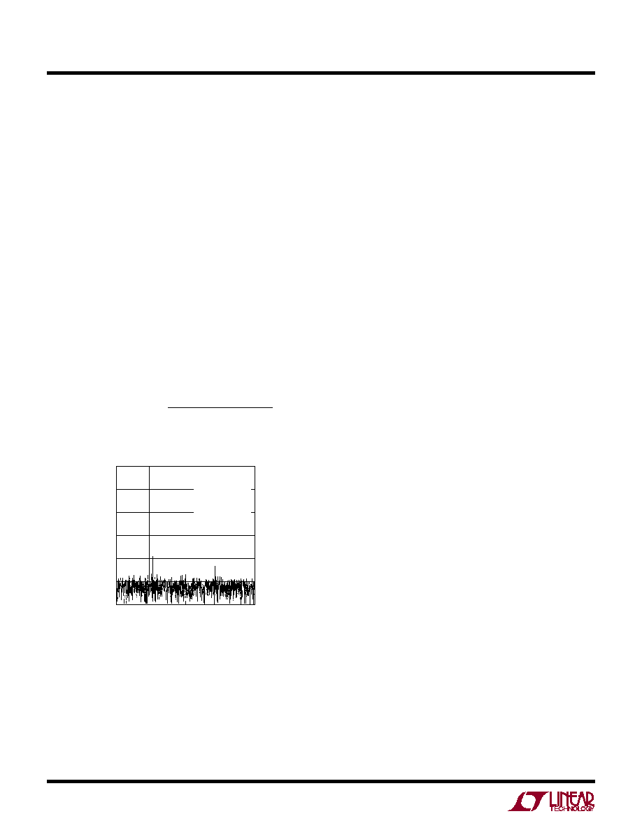
Figure 5 shows the IMD performance at a 20kHz input.
FREQUENCY (kHz)
0
–120
AMPLITUDE
(dB)
–100
–80
–60
–40
20
40
60
80
LTC1282 F05
–20
0
10
30
50
70
fSAMPLE = 160kHz
fIN1 = 19.0kHz
fIN2 = 20.6kHz
VDD = 3V
UNIPOLAR
Figure 5. Intermodulation Distortion Plot
Full Power and Full Linear Bandwidth
The full power bandwidth is that input frequency at which
the amplitude of the reconstructed fundamental is re-
duced by 3dB for a full-scale input signal.
The full linear bandwidth is the input frequency at which
the S/(N + D) has dropped to 68dB (11 effective bits). The
LTC1282 has been designed to optimize input bandwidth,
allowing the ADC to undersample input signals with fre-
quencies above the converter’s Nyquist Frequency.
Driving the Analog Input
The analog input of the LTC1282 is easy to drive. It draws
only one small current spike while charging the sample-
and-hold capacitor at the end of conversion. During con-
version the analog input draws no current. The only
requirement is that the amplifier driving the analog input
must settle after the small current spike before the next
conversion starts. Any op amp that settles in 1.14
s to
small current transients will allow maximum speed opera-
tion. If slower op amps are used, more settling time can be
provided by increasing the time between conversions.
Suitable devices capable of driving the ADC’s AIN input
include the LT
1190/LT1191, LT1007, LT1220, LT1223
and LT1224 op amps.
The analog input tolerates source resistance very well.
Here again, the only requirement is that the analog input
must settle before the next conversion starts. For larger
source resistance, full accuracy can be obtained if more
time is allowed between conversions.
Internal Reference
The LTC1282 has an on-chip, temperature compensated,
curvature corrected, bandgap reference which is factory
trimmed to 1.20V. It is internally connected to the DAC and
is available at pin 2 to provide up to 0.3mA current to an
external load.
For minimum code transition noise the reference output
should be decoupled with a capacitor to filter wideband
noise from the reference (10
F tantalum in parallel with a
0.1
F ceramic).
Peak Harmonic or Spurious Noise
The peak harmonic or spurious noise is the largest spec-
tral component excluding the input signal and DC. This
value is expressed in decibels relative to the RMS value of
a full-scale input signal.
相关PDF资料 |
PDF描述 |
|---|---|
| LTC1288IS8#TRPBF | IC A/D CONV SAMPLING 12BIT 8SOIC |
| LTC1298IS8#TRPBF | IC A/D CONV SAMPLING 12BIT 8SOIC |
| LTC1327CNW#PBF | IC TXRX EIA/TIA-562 3.3V 28-DIP |
| LTC1329ACS8-50#TRPBF | IC D/A CONV 8BIT MICROPWR 8-SOIC |
| LTC1337CNW#PBF | IC 3DVR/5RCVR 5V RS232 28-DIP |
相关代理商/技术参数 |
参数描述 |
|---|---|
| LTC1282ACSW | 功能描述:IC A/D CONV SAMPLING W/REF24SOIC RoHS:否 类别:集成电路 (IC) >> 数据采集 - 模数转换器 系列:- 标准包装:1,000 系列:- 位数:12 采样率(每秒):300k 数据接口:并联 转换器数目:1 功率耗散(最大):75mW 电压电源:单电源 工作温度:0°C ~ 70°C 安装类型:表面贴装 封装/外壳:24-SOIC(0.295",7.50mm 宽) 供应商设备封装:24-SOIC 包装:带卷 (TR) 输入数目和类型:1 个单端,单极;1 个单端,双极 |
| LTC1282ACSW#PBF | 功能描述:IC A/D CONV SAMPLING W/REF24SOIC RoHS:是 类别:集成电路 (IC) >> 数据采集 - 模数转换器 系列:- 标准包装:1,000 系列:- 位数:12 采样率(每秒):300k 数据接口:并联 转换器数目:1 功率耗散(最大):75mW 电压电源:单电源 工作温度:0°C ~ 70°C 安装类型:表面贴装 封装/外壳:24-SOIC(0.295",7.50mm 宽) 供应商设备封装:24-SOIC 包装:带卷 (TR) 输入数目和类型:1 个单端,单极;1 个单端,双极 |
| LTC1282ACSW#TR | 功能描述:IC ADC 12BIT SAMPLING REF 24SOIC RoHS:否 类别:集成电路 (IC) >> 数据采集 - 模数转换器 系列:- 标准包装:1,000 系列:- 位数:12 采样率(每秒):300k 数据接口:并联 转换器数目:1 功率耗散(最大):75mW 电压电源:单电源 工作温度:0°C ~ 70°C 安装类型:表面贴装 封装/外壳:24-SOIC(0.295",7.50mm 宽) 供应商设备封装:24-SOIC 包装:带卷 (TR) 输入数目和类型:1 个单端,单极;1 个单端,双极 |
| LTC1282ACSW#TRPBF | 功能描述:IC A/D CONV SAMPLING W/REF24SOIC RoHS:是 类别:集成电路 (IC) >> 数据采集 - 模数转换器 系列:- 标准包装:1,000 系列:- 位数:12 采样率(每秒):300k 数据接口:并联 转换器数目:1 功率耗散(最大):75mW 电压电源:单电源 工作温度:0°C ~ 70°C 安装类型:表面贴装 封装/外壳:24-SOIC(0.295",7.50mm 宽) 供应商设备封装:24-SOIC 包装:带卷 (TR) 输入数目和类型:1 个单端,单极;1 个单端,双极 |
| LTC1282BCN | 功能描述:IC A/D CONV SAMPLING W/REF 24DIP RoHS:否 类别:集成电路 (IC) >> 数据采集 - 模数转换器 系列:- 其它有关文件:TSA1204 View All Specifications 标准包装:1 系列:- 位数:12 采样率(每秒):20M 数据接口:并联 转换器数目:2 功率耗散(最大):155mW 电压电源:模拟和数字 工作温度:-40°C ~ 85°C 安装类型:表面贴装 封装/外壳:48-TQFP 供应商设备封装:48-TQFP(7x7) 包装:Digi-Reel® 输入数目和类型:4 个单端,单极;2 个差分,单极 产品目录页面:1156 (CN2011-ZH PDF) 其它名称:497-5435-6 |
发布紧急采购,3分钟左右您将得到回复。