- 您现在的位置:买卖IC网 > PDF目录9477 > LTC1289CCSW#PBF (Linear Technology)IC DATA ACQ SYS 12BIT 3V 20-SOIC PDF资料下载
参数资料
| 型号: | LTC1289CCSW#PBF |
| 厂商: | Linear Technology |
| 文件页数: | 15/28页 |
| 文件大小: | 0K |
| 描述: | IC DATA ACQ SYS 12BIT 3V 20-SOIC |
| 标准包装: | 38 |
| 类型: | 数据采集系统(DAS) |
| 分辨率(位): | 12 b |
| 采样率(每秒): | 25k |
| 数据接口: | 串行,并联 |
| 电压电源: | 双 ± |
| 电源电压: | ±3.3V |
| 工作温度: | 0°C ~ 70°C |
| 安装类型: | 表面贴装 |
| 封装/外壳: | 20-SOIC(0.295",7.50mm 宽) |
| 供应商设备封装: | 20-SOIC |
| 包装: | 管件 |
第1页第2页第3页第4页第5页第6页第7页第8页第9页第10页第11页第12页第13页第14页当前第15页第16页第17页第18页第19页第20页第21页第22页第23页第24页第25页第26页第27页第28页
22
LTC1289
1289fb
U
S
A
O
PPLICATI
WU
U
I FOR ATIO
Figure 19 shows an FFT plot of the output spectrum for two
tones applied to the input of the A/D. Nonlinearities in the
A/D will cause distortion products at the sum and differ-
ence frequencies of the fundamentals and products of the
fundamentals. This is classically referred to as
intermodulation distortion (IMD).
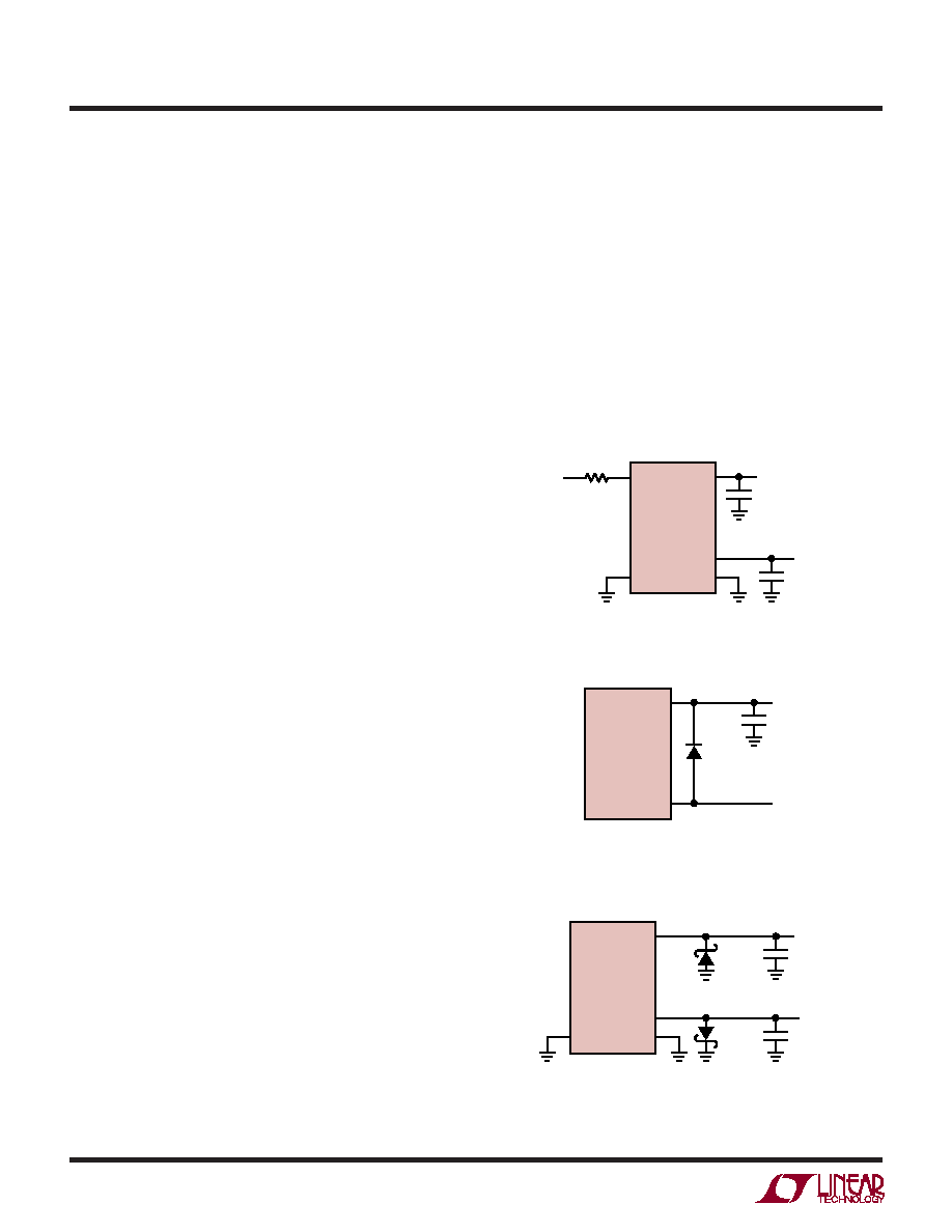
8. Overvoltage Protection
Applying signals to the analog MUX that exceed the
positive or negative supply of the device will degrade the
accuracy of the A/D and possibly damage the device. For
example this condition would occur if a signal is applied to
the analog MUX before power is applied to the LTC1289.
Another example is the input source is operating from
different supplies of larger value than the LTC1289. These
conditions should be prevented either with proper supply
sequencing or by use of external circuitry to clamp or
current limit the input source. As shown in Figure 20, a
1k
resistor is enough to stand off ±15V (15mA for one
only channel). If more than one channel exceeds the
supplies than the following guidelines can be used. Limit
the current to 7mA per channel and 28mA for all channels.
This means four channels can handle 7mA of input current
each. Reducing the ACLK and SCLK frequencies from the
maximum of 2MHz and 1MHz, respectively (see Typical
Peformance Characteristics curves Maximum ACLK Fre-
quency vs Source Resistance and Sample and Hold Acqui-
sition Time vs Source Resistance) allows the use of larger
current limiting resistors. Use 1N4148 diode clamps from
the MUX inputs to VCC and V – if the value of the series
resistor will not allow the maximum clock speeds to be
used or if an unknown source is used to drive the LTC1289
MUX inputs.
How the various power supplies to the LTC1289 are
applied can also lead to overvoltage conditions. For single
supply operation (i.e., unipolar mode), if VCC and REF+ are
not tied together, then VCC should be turned on first, then
REF+. If this sequence cannot be met, connecting a diode
from REF+ to VCC is recommended (see Figure 21).
For dual supplies (bipolar mode) placing two Schottky
diodes from VCC and V– to ground (Figure 22) will prevent
power supply reversal from occuring when an input source
is applied to the analog MUX before power is applied to the
device. Power supply reversal occurs, for example, if the
input is pulled below V– then VCC will pull a diode drop
below ground which could cause the device not to power
up properly. Likewise, if the input is pulled above VCC then
V– will be pulled a diode drop above ground. If no inputs
are present on the MUX, the Schottky diodes are not
required if V– is applied first, then VCC.
Because a unique input protection structure is used on the
digital input pins, the signal levels on these pins can
exceed the device VCC without damaging the device.
3.3V
LTC1289 AIF20
DGND
V–
AGND
VCC
1k
LTC1289
CH0
VIN
–3.3V
0.1
F
22
F
Figure 20. Overvoltage Protection for MUX
3.3V
LTC1289 AIF21
REF+
VCC
LTC1289
22
F
1N4148
VREF
14
20
Figure 21.
3.3V
LTC1289 AIF22
DGND
V –
AGND
VCC
LTC1289
–3.3V
0.1
F
22
F
1N5817
Figure 22. Power Supply Reversal
相关PDF资料 |
PDF描述 |
|---|---|
| LTC6905CS5-100#TRM | IC OSC SILICON 100MHZ TSOT23-5 |
| LTC1289CCSW | IC DATA ACQ SYS 12BIT 3V 20-SOIC |
| LTC1287BCN8 | IC DATA ACQ SYS 12BIT 3V 8-DIP |
| V110A5M200BF | CONVERTER MOD DC/DC 5V 200W |
| LTC1292BIN8#PBF | IC DATA ACQ SYSTEM 12BIT 8-DIP |
相关代理商/技术参数 |
参数描述 |
|---|---|
| LTC1290BCJ | 制造商:Linear Technology 功能描述:ADC Single SAR 50ksps 12-bit Serial 20-Pin CDIP |
| LTC1290BCN | 功能描述:IC DATA ACQ SYS 12BIT 20-DIP RoHS:否 类别:集成电路 (IC) >> 数据采集 - ADCs/DAC - 专用型 系列:- 产品培训模块:Lead (SnPb) Finish for COTS Obsolescence Mitigation Program 标准包装:50 系列:- 类型:数据采集系统(DAS) 分辨率(位):16 b 采样率(每秒):21.94k 数据接口:MICROWIRE?,QSPI?,串行,SPI? 电压电源:模拟和数字 电源电压:1.8 V ~ 3.6 V 工作温度:-40°C ~ 85°C 安装类型:表面贴装 封装/外壳:40-WFQFN 裸露焊盘 供应商设备封装:40-TQFN-EP(6x6) 包装:托盘 |
| LTC1290BCN#PBF | 功能描述:IC DATA ACQ SYS 12BIT 20-DIP RoHS:是 类别:集成电路 (IC) >> 数据采集 - ADCs/DAC - 专用型 系列:- 产品培训模块:Lead (SnPb) Finish for COTS Obsolescence Mitigation Program 标准包装:50 系列:- 类型:数据采集系统(DAS) 分辨率(位):16 b 采样率(每秒):21.94k 数据接口:MICROWIRE?,QSPI?,串行,SPI? 电压电源:模拟和数字 电源电压:1.8 V ~ 3.6 V 工作温度:-40°C ~ 85°C 安装类型:表面贴装 封装/外壳:40-WFQFN 裸露焊盘 供应商设备封装:40-TQFN-EP(6x6) 包装:托盘 |
| LTC1290BCSW | 功能描述:IC DATA ACQ SYS 12BIT 20-SOIC RoHS:否 类别:集成电路 (IC) >> 数据采集 - ADCs/DAC - 专用型 系列:- 产品培训模块:Lead (SnPb) Finish for COTS Obsolescence Mitigation Program 标准包装:50 系列:- 类型:数据采集系统(DAS) 分辨率(位):16 b 采样率(每秒):21.94k 数据接口:MICROWIRE?,QSPI?,串行,SPI? 电压电源:模拟和数字 电源电压:1.8 V ~ 3.6 V 工作温度:-40°C ~ 85°C 安装类型:表面贴装 封装/外壳:40-WFQFN 裸露焊盘 供应商设备封装:40-TQFN-EP(6x6) 包装:托盘 |
| LTC1290BCSW#PBF | 功能描述:IC DATA ACQ SYS 12BIT 20-SOIC RoHS:是 类别:集成电路 (IC) >> 数据采集 - ADCs/DAC - 专用型 系列:- 产品培训模块:Lead (SnPb) Finish for COTS Obsolescence Mitigation Program 标准包装:50 系列:- 类型:数据采集系统(DAS) 分辨率(位):16 b 采样率(每秒):21.94k 数据接口:MICROWIRE?,QSPI?,串行,SPI? 电压电源:模拟和数字 电源电压:1.8 V ~ 3.6 V 工作温度:-40°C ~ 85°C 安装类型:表面贴装 封装/外壳:40-WFQFN 裸露焊盘 供应商设备封装:40-TQFN-EP(6x6) 包装:托盘 |
发布紧急采购,3分钟左右您将得到回复。