- 您现在的位置:买卖IC网 > PDF目录39404 > LTC1289CIJ#PBF (LINEAR TECHNOLOGY CORP) 8-CH 12-BIT SUCCESSIVE APPROXIMATION ADC, SERIAL ACCESS, CDIP20 PDF资料下载
参数资料
| 型号: | LTC1289CIJ#PBF |
| 厂商: | LINEAR TECHNOLOGY CORP |
| 元件分类: | ADC |
| 英文描述: | 8-CH 12-BIT SUCCESSIVE APPROXIMATION ADC, SERIAL ACCESS, CDIP20 |
| 封装: | 0.300 INCH, LEAD FREE, CERDIP-20 |
| 文件页数: | 8/28页 |
| 文件大小: | 663K |
| 代理商: | LTC1289CIJ#PBF |
第1页第2页第3页第4页第5页第6页第7页当前第8页第9页第10页第11页第12页第13页第14页第15页第16页第17页第18页第19页第20页第21页第22页第23页第24页第25页第26页第27页第28页
16
LTC1289
1289fb
U
S
A
O
PPLICATI
WU
U
I FOR ATIO
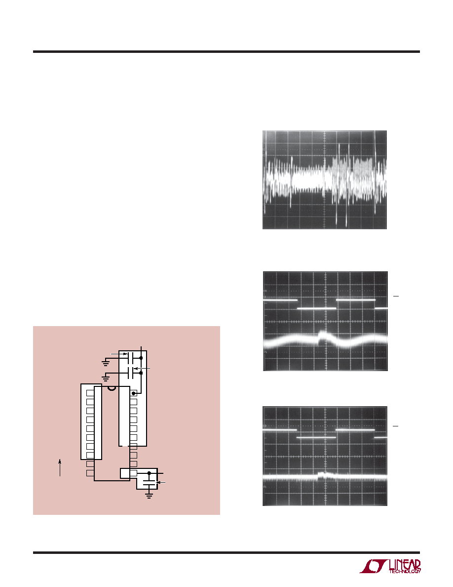
Figure 6 shows an example of an ideal ground plane design
for a two-sided board. Of course, this much ground plane
will not always be possible, but users should strive to get
as close to this ideal as possible.
2. Bypassing
For good performance, VCC must be free of noise and
ripple. Any changes in the VCC voltage with respect to
analog ground during a conversion cycle can induce
errors or noise in the output code. VCC noise and ripple can
be kept below 0.5mV by bypassing the VCC pin directly to
the analog ground plane with a 22
F tantalum capacitor
and leads as short as possible. The lead from the device to
the VCC supply should also be kept to a minimum and the
VCC supply should have a low output impedance such as
that obtained from a voltage regulator (e.g., LT1117).
Using a battery to power the LTC1289 will help reduce the
amount of bypass capacitance required on the VCC pin. A
battery placed close to the device will only require 10
F to
adequately bypass the supply pin. Figure 7 shows the
effect of poor VCC bypassing. Figure 8a shows the settling
of a LT1117 low dropout regulator with a 22
F bypass
capacitor. The noise and ripple is approximately 0.5mV.
Figure 8b shows the response of a lithium battery with a 10
F
bypass capacitor. The noise and ripple is kept below 0.5mV.
Figure 7. Poor VCC Bypassing.
Noise and Ripple Can Cause A/D Errors.
Figure 8a. LT1117 Regulator with 22
F Bypassing on VCC
HORIZONTAL: 20
s/DIV
5V/DIV
CS
0.5mV/DIV
VCC
Figure 8b. Lithium Battery with 10
F Bypassing on VCC
HORIZONTAL: 20
s/DIV
Figure 6. Example Ground Plane for the LTC1289
V–
22
F
TANTALUM
VCC
LTC1289 AIF06
0.1
F
CERAMIC
DISK
ANALOG
GROUND
PLANE
0.1
F
1
2
3
4
5
6
7
8
9
10
20
19
18
17
16
15
14
13
12
11
0.5mV/DIV
5V/DIV
CS
VCC
VERTICAL:
0.5mV/DIV
HORIZONTAL: 10
s/DIV
相关PDF资料 |
PDF描述 |
|---|---|
| LTC1289CIJ#TRPBF | 8-CH 12-BIT SUCCESSIVE APPROXIMATION ADC, SERIAL ACCESS, CDIP20 |
| LTC1289BCJ#TRPBF | 8-CH 12-BIT SUCCESSIVE APPROXIMATION ADC, SERIAL ACCESS, CDIP20 |
| LTC1289CIJ#TR | 8-CH 12-BIT SUCCESSIVE APPROXIMATION ADC, SERIAL ACCESS, CDIP20 |
| LTC1289CCN#TR | 8-CH 12-BIT SUCCESSIVE APPROXIMATION ADC, SERIAL ACCESS, PDIP20 |
| LTC1289BCJ#PBF | 8-CH 12-BIT SUCCESSIVE APPROXIMATION ADC, SERIAL ACCESS, CDIP20 |
相关代理商/技术参数 |
参数描述 |
|---|---|
| LTC1290BCJ | 制造商:Linear Technology 功能描述:ADC Single SAR 50ksps 12-bit Serial 20-Pin CDIP |
| LTC1290BCN | 功能描述:IC DATA ACQ SYS 12BIT 20-DIP RoHS:否 类别:集成电路 (IC) >> 数据采集 - ADCs/DAC - 专用型 系列:- 产品培训模块:Lead (SnPb) Finish for COTS Obsolescence Mitigation Program 标准包装:50 系列:- 类型:数据采集系统(DAS) 分辨率(位):16 b 采样率(每秒):21.94k 数据接口:MICROWIRE?,QSPI?,串行,SPI? 电压电源:模拟和数字 电源电压:1.8 V ~ 3.6 V 工作温度:-40°C ~ 85°C 安装类型:表面贴装 封装/外壳:40-WFQFN 裸露焊盘 供应商设备封装:40-TQFN-EP(6x6) 包装:托盘 |
| LTC1290BCN#PBF | 功能描述:IC DATA ACQ SYS 12BIT 20-DIP RoHS:是 类别:集成电路 (IC) >> 数据采集 - ADCs/DAC - 专用型 系列:- 产品培训模块:Lead (SnPb) Finish for COTS Obsolescence Mitigation Program 标准包装:50 系列:- 类型:数据采集系统(DAS) 分辨率(位):16 b 采样率(每秒):21.94k 数据接口:MICROWIRE?,QSPI?,串行,SPI? 电压电源:模拟和数字 电源电压:1.8 V ~ 3.6 V 工作温度:-40°C ~ 85°C 安装类型:表面贴装 封装/外壳:40-WFQFN 裸露焊盘 供应商设备封装:40-TQFN-EP(6x6) 包装:托盘 |
| LTC1290BCSW | 功能描述:IC DATA ACQ SYS 12BIT 20-SOIC RoHS:否 类别:集成电路 (IC) >> 数据采集 - ADCs/DAC - 专用型 系列:- 产品培训模块:Lead (SnPb) Finish for COTS Obsolescence Mitigation Program 标准包装:50 系列:- 类型:数据采集系统(DAS) 分辨率(位):16 b 采样率(每秒):21.94k 数据接口:MICROWIRE?,QSPI?,串行,SPI? 电压电源:模拟和数字 电源电压:1.8 V ~ 3.6 V 工作温度:-40°C ~ 85°C 安装类型:表面贴装 封装/外壳:40-WFQFN 裸露焊盘 供应商设备封装:40-TQFN-EP(6x6) 包装:托盘 |
| LTC1290BCSW#PBF | 功能描述:IC DATA ACQ SYS 12BIT 20-SOIC RoHS:是 类别:集成电路 (IC) >> 数据采集 - ADCs/DAC - 专用型 系列:- 产品培训模块:Lead (SnPb) Finish for COTS Obsolescence Mitigation Program 标准包装:50 系列:- 类型:数据采集系统(DAS) 分辨率(位):16 b 采样率(每秒):21.94k 数据接口:MICROWIRE?,QSPI?,串行,SPI? 电压电源:模拟和数字 电源电压:1.8 V ~ 3.6 V 工作温度:-40°C ~ 85°C 安装类型:表面贴装 封装/外壳:40-WFQFN 裸露焊盘 供应商设备封装:40-TQFN-EP(6x6) 包装:托盘 |
发布紧急采购,3分钟左右您将得到回复。