- 您现在的位置:买卖IC网 > PDF目录39404 > LTC1290CIJ#PBF (LINEAR TECHNOLOGY CORP) 8-CH 12-BIT SUCCESSIVE APPROXIMATION ADC, SERIAL ACCESS, CDIP20 PDF资料下载
参数资料
| 型号: | LTC1290CIJ#PBF |
| 厂商: | LINEAR TECHNOLOGY CORP |
| 元件分类: | ADC |
| 英文描述: | 8-CH 12-BIT SUCCESSIVE APPROXIMATION ADC, SERIAL ACCESS, CDIP20 |
| 封装: | 0.300 INCH, LEAD FREE, HERMETIC SEALED, CERAMIC, DIP-20 |
| 文件页数: | 5/32页 |
| 文件大小: | 613K |
| 代理商: | LTC1290CIJ#PBF |
第1页第2页第3页第4页当前第5页第6页第7页第8页第9页第10页第11页第12页第13页第14页第15页第16页第17页第18页第19页第20页第21页第22页第23页第24页第25页第26页第27页第28页第29页第30页第31页第32页
13
LTC1290
1290fe
U
S
A
O
PPLICATI
WU
U
I FOR ATIO
MSB-First/LSB-First Format (MSBF)
The output data of the LTC1290 is programmed for MSB-
first or LSB-first sequence using the MSBF bit. For MSB
first output data the input word clocked to the LTC1290
should always contain a logical one in the sixth bit location
(MSBF bit). Likewise for LSB-first output data the input
word clocked to the LTC1290 should always contain a zero
in the MSBF bit location. The MSBF bit affects only the
order of the output data word. The order of the input word
is unaffected by this bit.
MSBF
OUTPUT FORMAT
0
LSB First
1
MSB First
Word Length (WL1, WL0) and Power Shutdown
The last two bits of the input word (WL1 and WL0)
program the output data word length and the power
shutdown feature of the LTC1290. Word lengths of 8, 12
or 16 bits can be selected according to the following table.
The WL1 and WL0 bits in a given DIN word control the
length of the present, not the next, DOUT word. WL1 and
WL0 are never “don’t cares” and must be set for the
correct DOUT word length even when a “dummy” DIN word
is sent. On any transfer cycle, the word length should be
made equal to the number of SCLK cycles sent by the
MPU. Power down will occur when WL1 = 0 and WL0 = 1
is selected. The previous conversion result will be clocked
out as a 10 bit word so a “dummy” conversion is required
before powering down the LTC1290. Conversions are
resumed once CS goes low or an SCLK is applied, if CS is
already low.
WL1
WL0
OUTPUT WORD LENGTH
0
8-Bits
0
1
Power Shutdown
1
0
12-Bits
1
16-Bits
Deglitcher
A deglitching circuit has been added to the Chip Select
input of the LTC1290 to minimize the effects of errors
caused by noise on that input. This circuit ignores changes
in state on the CS input that are shorter in duration than
one ACLK cycle. After a change of state on the CS input, the
LTC1290 waits for two falling edge of the ACLK before
recognizing a valid chip select. One indication of CS
recognition is the DOUT line becoming active (leaving the
Hi-Z state). Note that the deglitching applies to both the
rising and falling CS edges.
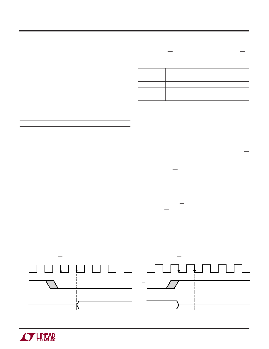
CS Low During Conversion
In the normal mode of operation, CS is brought high
during the conversion time. The serial port ignores any
SCLK activity while CS is high. The LTC1290 will also
operate with CS low during the conversion. In this mode,
SCLK must remain low during the conversion as shown in
the following figure. After the conversion is complete, the
DOUT line will become active with the first output bit. Then
the data transfer can begin as normal.
Low CS Recognized Internally
High CS Recognized Internally
DOUT
CS
LTC1290 AI07
ACLK
VALID OUTPUT
HI-Z
DOUT
CS
LTC1290 AI06
ACLK
VALID OUTPUT
HI-Z
相关PDF资料 |
PDF描述 |
|---|---|
| LTC1290DMJ#TR | 8-CH 12-BIT SUCCESSIVE APPROXIMATION ADC, SERIAL ACCESS, CDIP20 |
| LTC1290DMJ#TRPBF | 8-CH 12-BIT SUCCESSIVE APPROXIMATION ADC, SERIAL ACCESS, CDIP20 |
| LTC1290CIN#TR | 8-CH 12-BIT SUCCESSIVE APPROXIMATION ADC, SERIAL ACCESS, PDIP20 |
| LTC1290DCN#TRPBF | 8-CH 12-BIT SUCCESSIVE APPROXIMATION ADC, SERIAL ACCESS, PDIP20 |
| LTC1290CIN#TRPBF | 8-CH 12-BIT SUCCESSIVE APPROXIMATION ADC, SERIAL ACCESS, PDIP20 |
相关代理商/技术参数 |
参数描述 |
|---|---|
| LTC1290CIN | 功能描述:IC DATA ACQ SYS 12BIT 20-DIP RoHS:否 类别:集成电路 (IC) >> 数据采集 - ADCs/DAC - 专用型 系列:- 产品培训模块:Lead (SnPb) Finish for COTS Obsolescence Mitigation Program 标准包装:50 系列:- 类型:数据采集系统(DAS) 分辨率(位):16 b 采样率(每秒):21.94k 数据接口:MICROWIRE?,QSPI?,串行,SPI? 电压电源:模拟和数字 电源电压:1.8 V ~ 3.6 V 工作温度:-40°C ~ 85°C 安装类型:表面贴装 封装/外壳:40-WFQFN 裸露焊盘 供应商设备封装:40-TQFN-EP(6x6) 包装:托盘 |
| LTC1290CIN#PBF | 功能描述:IC DATA ACQ SYS 12BIT 20-DIP RoHS:是 类别:集成电路 (IC) >> 数据采集 - ADCs/DAC - 专用型 系列:- 产品培训模块:Lead (SnPb) Finish for COTS Obsolescence Mitigation Program 标准包装:50 系列:- 类型:数据采集系统(DAS) 分辨率(位):16 b 采样率(每秒):21.94k 数据接口:MICROWIRE?,QSPI?,串行,SPI? 电压电源:模拟和数字 电源电压:1.8 V ~ 3.6 V 工作温度:-40°C ~ 85°C 安装类型:表面贴装 封装/外壳:40-WFQFN 裸露焊盘 供应商设备封装:40-TQFN-EP(6x6) 包装:托盘 |
| LTC1290CISW | 功能描述:IC DATA ACQ SYS 12BIT 20-SOIC RoHS:否 类别:集成电路 (IC) >> 数据采集 - ADCs/DAC - 专用型 系列:- 产品培训模块:Lead (SnPb) Finish for COTS Obsolescence Mitigation Program 标准包装:50 系列:- 类型:数据采集系统(DAS) 分辨率(位):16 b 采样率(每秒):21.94k 数据接口:MICROWIRE?,QSPI?,串行,SPI? 电压电源:模拟和数字 电源电压:1.8 V ~ 3.6 V 工作温度:-40°C ~ 85°C 安装类型:表面贴装 封装/外壳:40-WFQFN 裸露焊盘 供应商设备封装:40-TQFN-EP(6x6) 包装:托盘 |
| LTC1290CISW#PBF | 功能描述:IC DATA ACQ SYS 12BIT 20-SOIC RoHS:是 类别:集成电路 (IC) >> 数据采集 - ADCs/DAC - 专用型 系列:- 产品培训模块:Data Converter Basics 标准包装:1 系列:- 类型:电机控制 分辨率(位):12 b 采样率(每秒):1M 数据接口:串行,并联 电压电源:单电源 电源电压:2.7 V ~ 3.6 V,4.5 V ~ 5.5 V 工作温度:-40°C ~ 85°C 安装类型:表面贴装 封装/外壳:100-TQFP 供应商设备封装:100-TQFP(14x14) 包装:剪切带 (CT) 其它名称:296-18373-1 |
| LTC1290CISW#PBF | 制造商:Linear Technology 功能描述:ADC, 8CH, 12BIT, 50KSPS, SOIC-20 |
发布紧急采购,3分钟左右您将得到回复。