- 您现在的位置:买卖IC网 > PDF目录39404 > LTC1290CIN#TR (LINEAR TECHNOLOGY CORP) 8-CH 12-BIT SUCCESSIVE APPROXIMATION ADC, SERIAL ACCESS, PDIP20 PDF资料下载
参数资料
| 型号: | LTC1290CIN#TR |
| 厂商: | LINEAR TECHNOLOGY CORP |
| 元件分类: | ADC |
| 英文描述: | 8-CH 12-BIT SUCCESSIVE APPROXIMATION ADC, SERIAL ACCESS, PDIP20 |
| 封装: | 0.300 INCH, PLASTIC, DIP-20 |
| 文件页数: | 28/32页 |
| 文件大小: | 613K |
| 代理商: | LTC1290CIN#TR |
第1页第2页第3页第4页第5页第6页第7页第8页第9页第10页第11页第12页第13页第14页第15页第16页第17页第18页第19页第20页第21页第22页第23页第24页第25页第26页第27页当前第28页第29页第30页第31页第32页
5
LTC1290
1290fe
LTC1290B/LTC1290C/LTC1290D
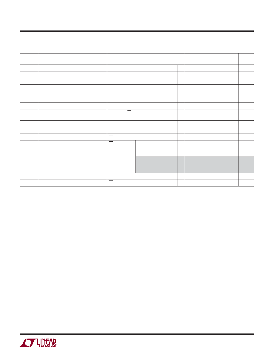
SYMBOL
PARAMETER
CONDITIONS
MIN
TYP
MAX
UNITS
VIH
High Level Input Voltage
VCC = 5.25V
●
2.0
V
VIL
Low Level Input Voltage
VCC = 4.75V
●
0.8
V
IIH
High Level Input Current
VIN = VCC
●
2.5
A
IIL
Low Level Input Current
VIN = 0V
●
– 2.5
A
VOH
High Level Output Voltage
VCC = 4.75V
IO = 10
A
4.7
V
IO = 360
A
●
2.4
4.0
V
VOL
Low Level Output Voltage
VCC = 4.75V
IO = 1.6mA
●
0.4
V
IOZ
High-Z Output Leakage
VOUT = VCC, CS High
●
3
A
VOUT = 0V, CS High
●
–3
A
ISOURCE
Output Source Current
VOUT = 0V
–20
mA
ISINK
Output Sink Current
VOUT = VCC
20
mA
ICC
Positive Supply Current
CS High
●
612
mA
CS High
LTC1290BC, LTC1290CC
●
510
A
Power Shutdown LTC1290DC, LTC1290BI
ACLK Off
LTC1290CI, LTC1290DI
LTC1290BM, LTC1290CM
●
515
A
LTC1290DM
(OBSOLETE)
IREF
Reference Current
VREF = 5V
●
10
50
A
I–
Negative Supply Current
CS High
●
150
A
VCC levels (4.5V), as high level reference or analog inputs (5V) can cause
this input diode to conduct, especially at elevated temperatures and cause
errors for inputs near full scale. This spec allows 50mV forward bias of
either diode. This means that as long as the reference or analog input does
not exceed the supply voltage by more than 50mV, the output code will be
correct. To achieve an absolute 0V to 5V input voltage range will therefore
require a minimum supply voltage of 4.950V over initial tolerance,
temperature variations and loading.
Note 8: Channel leakage current is measured after the channel selection.
Note 9: To minimize errors caused by noise at the chip select input, the
internal circuitry waits for two ACLK falling edge after a chip select falling
edge is detected before responding to control input signals. Therefore, no
attempt should be made to clock an address in or data out until the
minimum chip select setup time has elapsed.
Note 10: Increased leakage currents at elevated temperatures cause the
S/H to droop, therefore it's recommended that fACLK ≥ 125kHz at 85°C and
fACLK ≥ 15kHz at 25°C.
Note 1: Absolute Maximum Ratings are those values beyond which the life
of a device may be impaired.
Note 2: All voltage values are with respect to ground with DGND, AGND
and REF
– wired together (unless otherwise noted).
Note 3: VCC = 5V, VREF+ = 5V, VREF – = 0V, V– = 0V for unipolar mode and
– 5V for bipolar mode, ACLK = 4.0MHz unless otherwise specified.
Note 4: These specs apply for both unipolar and bipolar modes. In bipolar
mode, one LSB is equal to the bipolar input span (2VREF) divided by 4096.
For example, when VREF = 5V, 1LSB (bipolar) = 2(5V)/4096 = 2.44mV.
Note 5: Integral nonlinearity is defined as the deviation of a code from a
straight line passing through the actual endpoints of the transfer curve.
The deviation is measured from the center of the quantization band.
Note 6: Recommended operating conditions.
Note 7: Two on-chip diodes are tied to each reference and analog input
which will conduct for reference or analog input voltages one diode drop
below V – or one diode drop above VCC. Be careful during testing at low
ELECTRICAL C
C
HARA TER STICS
DIGITAL A D
U
I
DC
The
● denotes the specifications which
apply over the full operating temperature range, otherwise specifications are at TA = 25°C. (Note 3)
相关PDF资料 |
PDF描述 |
|---|---|
| LTC1290DCN#TRPBF | 8-CH 12-BIT SUCCESSIVE APPROXIMATION ADC, SERIAL ACCESS, PDIP20 |
| LTC1290CIN#TRPBF | 8-CH 12-BIT SUCCESSIVE APPROXIMATION ADC, SERIAL ACCESS, PDIP20 |
| LTC1290BMJ#PBF | 8-CH 12-BIT SUCCESSIVE APPROXIMATION ADC, SERIAL ACCESS, CDIP20 |
| LTC1290CCN#TRPBF | 8-CH 12-BIT SUCCESSIVE APPROXIMATION ADC, SERIAL ACCESS, PDIP20 |
| LTC1290BMJ#TRPBF | 8-CH 12-BIT SUCCESSIVE APPROXIMATION ADC, SERIAL ACCESS, CDIP20 |
相关代理商/技术参数 |
参数描述 |
|---|---|
| LTC1290CISW | 功能描述:IC DATA ACQ SYS 12BIT 20-SOIC RoHS:否 类别:集成电路 (IC) >> 数据采集 - ADCs/DAC - 专用型 系列:- 产品培训模块:Lead (SnPb) Finish for COTS Obsolescence Mitigation Program 标准包装:50 系列:- 类型:数据采集系统(DAS) 分辨率(位):16 b 采样率(每秒):21.94k 数据接口:MICROWIRE?,QSPI?,串行,SPI? 电压电源:模拟和数字 电源电压:1.8 V ~ 3.6 V 工作温度:-40°C ~ 85°C 安装类型:表面贴装 封装/外壳:40-WFQFN 裸露焊盘 供应商设备封装:40-TQFN-EP(6x6) 包装:托盘 |
| LTC1290CISW#PBF | 功能描述:IC DATA ACQ SYS 12BIT 20-SOIC RoHS:是 类别:集成电路 (IC) >> 数据采集 - ADCs/DAC - 专用型 系列:- 产品培训模块:Data Converter Basics 标准包装:1 系列:- 类型:电机控制 分辨率(位):12 b 采样率(每秒):1M 数据接口:串行,并联 电压电源:单电源 电源电压:2.7 V ~ 3.6 V,4.5 V ~ 5.5 V 工作温度:-40°C ~ 85°C 安装类型:表面贴装 封装/外壳:100-TQFP 供应商设备封装:100-TQFP(14x14) 包装:剪切带 (CT) 其它名称:296-18373-1 |
| LTC1290CISW#PBF | 制造商:Linear Technology 功能描述:ADC, 8CH, 12BIT, 50KSPS, SOIC-20 |
| LTC1290CISW#TR | 功能描述:IC DATA ACQ SYS 12BIT 5V 20SOIC RoHS:否 类别:集成电路 (IC) >> 数据采集 - ADCs/DAC - 专用型 系列:- 产品培训模块:Lead (SnPb) Finish for COTS Obsolescence Mitigation Program 标准包装:50 系列:- 类型:数据采集系统(DAS) 分辨率(位):16 b 采样率(每秒):21.94k 数据接口:MICROWIRE?,QSPI?,串行,SPI? 电压电源:模拟和数字 电源电压:1.8 V ~ 3.6 V 工作温度:-40°C ~ 85°C 安装类型:表面贴装 封装/外壳:40-WFQFN 裸露焊盘 供应商设备封装:40-TQFN-EP(6x6) 包装:托盘 |
| LTC1290CISW#TRPBF | 功能描述:IC DATA ACQ SYS 12BIT 20-SOIC RoHS:是 类别:集成电路 (IC) >> 数据采集 - ADCs/DAC - 专用型 系列:- 产品培训模块:Lead (SnPb) Finish for COTS Obsolescence Mitigation Program 标准包装:50 系列:- 类型:数据采集系统(DAS) 分辨率(位):16 b 采样率(每秒):21.94k 数据接口:MICROWIRE?,QSPI?,串行,SPI? 电压电源:模拟和数字 电源电压:1.8 V ~ 3.6 V 工作温度:-40°C ~ 85°C 安装类型:表面贴装 封装/外壳:40-WFQFN 裸露焊盘 供应商设备封装:40-TQFN-EP(6x6) 包装:托盘 |
发布紧急采购,3分钟左右您将得到回复。