- 您现在的位置:买卖IC网 > PDF目录9476 > LTC1290CISW#TRPBF (Linear Technology)IC DATA ACQ SYS 12BIT 20-SOIC PDF资料下载
参数资料
| 型号: | LTC1290CISW#TRPBF |
| 厂商: | Linear Technology |
| 文件页数: | 22/32页 |
| 文件大小: | 0K |
| 描述: | IC DATA ACQ SYS 12BIT 20-SOIC |
| 标准包装: | 1,000 |
| 类型: | 数据采集系统(DAS),ADC |
| 分辨率(位): | 12 b |
| 采样率(每秒): | 50k |
| 数据接口: | 串行,并联 |
| 电压电源: | 双 ± |
| 电源电压: | ±5 V,5 V |
| 工作温度: | -40°C ~ 85°C |
| 安装类型: | 表面贴装 |
| 封装/外壳: | 20-SOIC(0.295",7.50mm 宽) |
| 供应商设备封装: | 20-SOIC |
| 包装: | 带卷 (TR) |
第1页第2页第3页第4页第5页第6页第7页第8页第9页第10页第11页第12页第13页第14页第15页第16页第17页第18页第19页第20页第21页当前第22页第23页第24页第25页第26页第27页第28页第29页第30页第31页第32页
29
LTC1290
1290fe
U
S
A
O
PPLICATI
TYPICAL
Power Shutdown
For battery-powered applications it is desirable to keep
power dissipation at a minimum. The LTC1290 can be
powered down when not in use reducing the supply
current from a nominal value of 5mA to typically 5
A (with
ACLK turned off). See the curve for Supply Current (Power
Shutdown) vs ACLK if ACLK cannot be turned off when the
LTC1290 is powered down. In this case the supply current
is proportional to the ACLK frequency and is independent
of temperature until it reaches the magnitude of the supply
current attained with ACLK turned off.
As an example of how to use this feature let’s add this to
the previous application, SNEAK-A-BIT. After the CHK
SIGN subroutine call insert the following:
JSR CHK SIGN
Determines which reading has valid
data, converts to 2’s complement
and stores in RAM
JSR SHUTDOWN
LTC1290 power shutdown routine
The actual subroutine is:
SHUTDOWN: LDA #$3D
Load DIN word for
LTC1290 into ACC
JSR TRANSFER Read LTC1290 routine
RTS
Return
To place the device in power shutdown the word length
bits are set to WL1 = 0 and WL0 = 1. The LTC1290 is
powered up on the next request for a conversion and it’s
ready to digitize an input signal immediately.
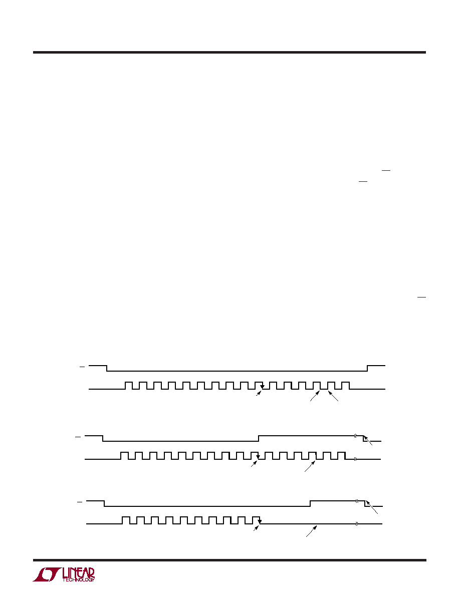
Power Shutdown Timing Considerations
After power shutdown has been requested, the LTC1290
is powered up on the next request for a conversion. This
request can be initiated either by bringing CS low or by
starting the next cycle of SCLKs if CS is kept low (see
Figures 3 and 4). When the SCLK frequency is much
slower than the ACLK frequency a situation can arise
where the LTC1290 could power down and then prema-
turely power back up. Power shutdown begins at the
negative going edge of the 10th SCLK once it has been
requested. A dummy conversion is executed and the
LTC1290 waits for the next request for conversion. If the
SCLKs have not finished once the LTC1290 has finished its
dummy conversion, it will recognize the next remaining
SCLKs as a request to start a conversion and power up the
LTC1290 (see Figure 23). To prevent this, bring either CS
high at the 10th SCLK (Figure 24) or clock out only 10
SCLKs (Figure 25) when power shutdown is requested.
110
SCLK
CS
POWER SHUTDOWN STARTS
DUMMY CONVERSION FINISHES AFTER 52 ACLK PERIODS
POWER UP
1290 TAF23
Figure 23. Power Shutdown Timing Problem
110
SCLK
CS
POWER SHUTDOWN STARTS
DUMMY CONVERSION FINISHES AFTER 52 ACLK PERIODS
POWER UP
1290 TAF24
Figure 24. Power Shutdown Timing
110
SCLK
CS
POWER SHUTDOWN STARTS
DUMMY CONVERSION FINISHES AFTER 52 ACLK PERIODS
POWER UP
1290 TAF25
Figure 25. Power Shutdown Timing
相关PDF资料 |
PDF描述 |
|---|---|
| MS27474T8F98PA | CONN RCPT 3POS JAM NUT W/PINS |
| VE-B1F-IU-F4 | CONVERTER MOD DC/DC 72V 200W |
| LTC1290CISW#TR | IC DATA ACQ SYS 12BIT 5V 20SOIC |
| VE-B1F-IU-F2 | CONVERTER MOD DC/DC 72V 200W |
| MS27473E16B6P | CONN PLUG 6POS STRAIGHT W/PINS |
相关代理商/技术参数 |
参数描述 |
|---|---|
| LTC1290CMJ | 制造商:Linear Technology 功能描述:ADC Single SAR 50ksps 12-bit Serial 20-Pin CDIP |
| LTC1290CMJ/883 | 制造商:Linear Technology 功能描述:ADC Single SAR 50ksps 12-bit Serial 20-Pin CDIP |
| LTC1290DCJ | 制造商:Linear Technology 功能描述:ADC Single SAR 50ksps 12-bit Serial 20-Pin CDIP |
| LTC1290DCN | 功能描述:IC DATA ACQ SYS 12BIT 20-DIP RoHS:否 类别:集成电路 (IC) >> 数据采集 - ADCs/DAC - 专用型 系列:- 产品培训模块:Lead (SnPb) Finish for COTS Obsolescence Mitigation Program 标准包装:50 系列:- 类型:数据采集系统(DAS) 分辨率(位):16 b 采样率(每秒):21.94k 数据接口:MICROWIRE?,QSPI?,串行,SPI? 电压电源:模拟和数字 电源电压:1.8 V ~ 3.6 V 工作温度:-40°C ~ 85°C 安装类型:表面贴装 封装/外壳:40-WFQFN 裸露焊盘 供应商设备封装:40-TQFN-EP(6x6) 包装:托盘 |
| LTC1290DCN#PBF | 功能描述:IC DATA ACQ SYS 12BIT 20-DIP RoHS:是 类别:集成电路 (IC) >> 数据采集 - ADCs/DAC - 专用型 系列:- 产品培训模块:Data Converter Basics 标准包装:1 系列:- 类型:电机控制 分辨率(位):12 b 采样率(每秒):1M 数据接口:串行,并联 电压电源:单电源 电源电压:2.7 V ~ 3.6 V,4.5 V ~ 5.5 V 工作温度:-40°C ~ 85°C 安装类型:表面贴装 封装/外壳:100-TQFP 供应商设备封装:100-TQFP(14x14) 包装:剪切带 (CT) 其它名称:296-18373-1 |
发布紧急采购,3分钟左右您将得到回复。