参数资料
| 型号: | LTC1293DCN |
| 厂商: | Linear Technology |
| 文件页数: | 10/28页 |
| 文件大小: | 0K |
| 描述: | IC DATA ACQ SYSTEM 12BIT 16-DIP |
| 标准包装: | 25 |
| 类型: | 数据采集系统(DAS),ADC |
| 分辨率(位): | 12 b |
| 采样率(每秒): | 46.5k |
| 数据接口: | 串行,并联 |
| 电压电源: | 双 ± |
| 电源电压: | ±5V,5V |
| 工作温度: | 0°C ~ 70°C |
| 安装类型: | 通孔 |
| 封装/外壳: | 16-DIP(0.300",7.62mm) |
| 供应商设备封装: | 16-PDIP |
| 包装: | 管件 |
第1页第2页第3页第4页第5页第6页第7页第8页第9页当前第10页第11页第12页第13页第14页第15页第16页第17页第18页第19页第20页第21页第22页第23页第24页第25页第26页第27页第28页
18
LTC1293/LTC1294/LTC1296
129346fs
U
S
A
O
PPLICATI
WU
U
I FOR ATIO
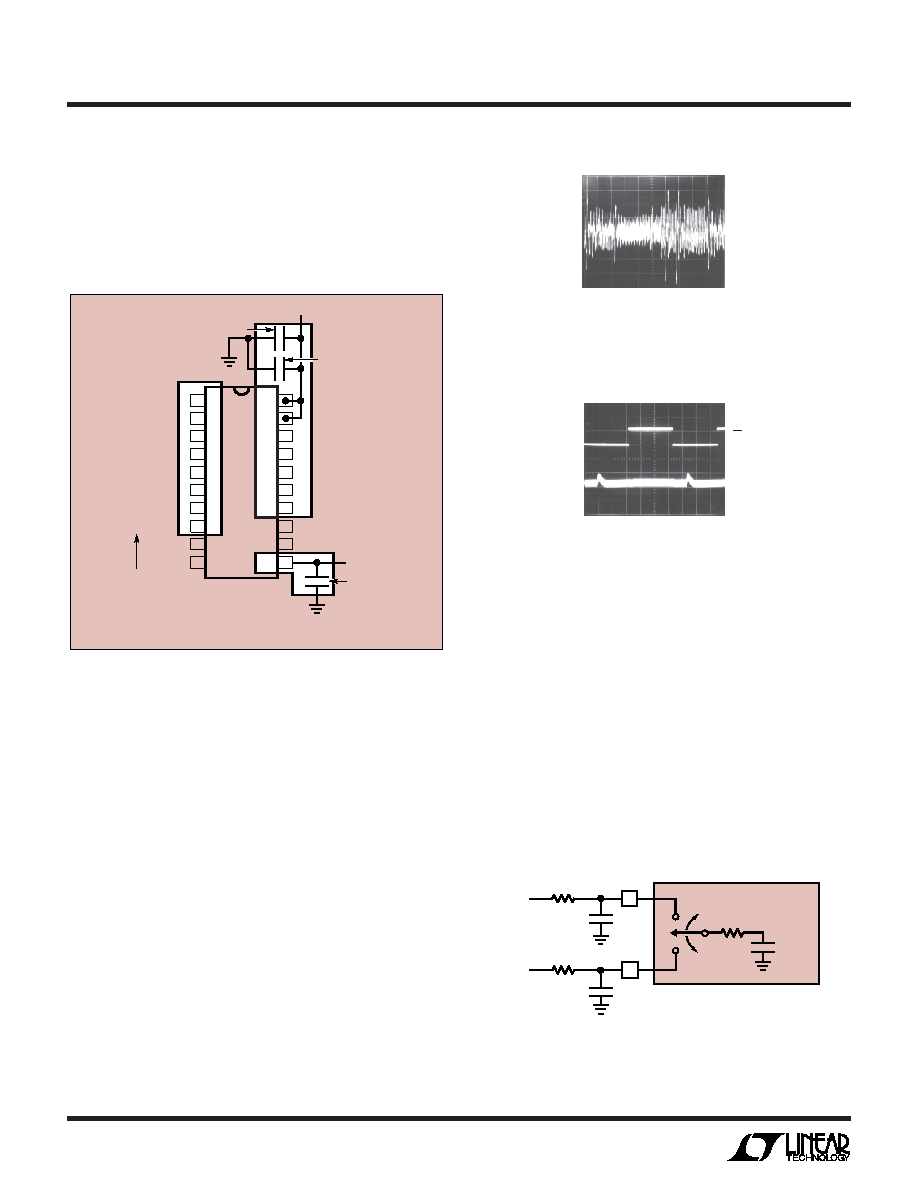
LTC1294. Figure 4 shows an example of an ideal LTC1293/
4/6 ground plane design for a two sided board. Of course
this much ground plane will not always be possible, but
users should strive to get as close to this ideal as possible.
Bypassing
For good performance, VCC must be free of noise and
ripple. Any changes in the VCC voltage with respect to
ground during a conversion cycle can induce errors or
noise in the output code. VCC noise and ripple can be kept
below 0.5mV by bypassing the VCC pin directly to the
analog ground plane with a minimum of 22
F tantalum
capacitor and with leads as short as possible. The lead
from the device to the VCC supply also should be kept to a
minimum and the VCC supply should have a low output
impedance such as obtained from a voltage regulator
(e.g., LT323A). For high frequency bypassing a 0.1
F
ceramic disk placed in parallel with the 22
F is recom-
mended. Again the leads should be kept to a minimum.
Figure 5 and 6 show the effects of good and poor VCC
bypassing.
HORIZONTAL: 10
s/DIV
VERTICAL:
0.5mV/DIV
VERTICAL:
0.5mV/DIV
HORIZONTAL: 10
s/DIV
Figure 5. Poor VCC Bypassing.
Noise and Ripple Can Cause A/D Errors.
Figure 6. Good VCC Bypassing Keeps Noise
and Ripple on VCC Below 1mV
CS
VCC
Analog Inputs
Because of the capacitive redistribution A/D conversion
techniques used, the analog inputs of the LTC1293/4/6
have capacitive switching input current spikes. These
current spikes settle quickly and do not cause a problem.
If large source resistances are used or if slow settling op
amps drive the inputs, take care to insure the transients
caused by the current spikes settle completely before the
conversion begins.
Figure 4. Ground Plane for the LTC1293/4/6
Figure 7. Analog Input Equivalent Circuit
6TH CLK
↑
RON = 500
8TH CLK
↓
CIN =
100pF
LTC1293/4/6
“+”
INPUT
RSOURCE +
VIN +
C1
“–”
INPUT
RSOURCE –
VIN –
C2
LTC1293 F07
V–
22
F
TANTALUM
VCC
LTC1293 F04
0.1
F
CERAMIC
DISK
ANALOG
GROUND
PLANE
0.1
F
CERAMIC
1
2
3
4
5
6
7
8
9
10
20
19
18
17
16
15
14
13
12
11
相关PDF资料 |
PDF描述 |
|---|---|
| LTC1292DCN8 | IC DATA ACQ SYSTEM 12BIT 8-DIP |
| M83723/82W1814N | CONN RCPT 14POS WALL MT W/SCKT |
| LTC1291DCN8 | IC DATA ACQ SYSTEM 12BIT 8-DIP |
| DS4125D+ | IC OSC CLOCK 125MHZ 10-LCCC |
| LTC1296CCN#PBF | IC DATA ACQ SYSTEM 12BIT 20-DIP |
相关代理商/技术参数 |
参数描述 |
|---|---|
| LTC1293DCN#PBF | 功能描述:IC DATA ACQ SYSTEM 12BIT 16-DIP RoHS:是 类别:集成电路 (IC) >> 数据采集 - ADCs/DAC - 专用型 系列:- 产品培训模块:Data Converter Basics 标准包装:1 系列:- 类型:电机控制 分辨率(位):12 b 采样率(每秒):1M 数据接口:串行,并联 电压电源:单电源 电源电压:2.7 V ~ 3.6 V,4.5 V ~ 5.5 V 工作温度:-40°C ~ 85°C 安装类型:表面贴装 封装/外壳:100-TQFP 供应商设备封装:100-TQFP(14x14) 包装:剪切带 (CT) 其它名称:296-18373-1 |
| LTC1293DCSW | 功能描述:IC DATA ACQ SYSTEM 12BIT 16-SOIC RoHS:否 类别:集成电路 (IC) >> 数据采集 - ADCs/DAC - 专用型 系列:- 产品培训模块:Lead (SnPb) Finish for COTS Obsolescence Mitigation Program 标准包装:50 系列:- 类型:数据采集系统(DAS) 分辨率(位):16 b 采样率(每秒):21.94k 数据接口:MICROWIRE?,QSPI?,串行,SPI? 电压电源:模拟和数字 电源电压:1.8 V ~ 3.6 V 工作温度:-40°C ~ 85°C 安装类型:表面贴装 封装/外壳:40-WFQFN 裸露焊盘 供应商设备封装:40-TQFN-EP(6x6) 包装:托盘 |
| LTC1293DCSW#PBF | 功能描述:IC DATA ACQ SYSTEM 12BIT 16-SOIC RoHS:是 类别:集成电路 (IC) >> 数据采集 - ADCs/DAC - 专用型 系列:- 产品培训模块:Data Converter Basics 标准包装:1 系列:- 类型:电机控制 分辨率(位):12 b 采样率(每秒):1M 数据接口:串行,并联 电压电源:单电源 电源电压:2.7 V ~ 3.6 V,4.5 V ~ 5.5 V 工作温度:-40°C ~ 85°C 安装类型:表面贴装 封装/外壳:100-TQFP 供应商设备封装:100-TQFP(14x14) 包装:剪切带 (CT) 其它名称:296-18373-1 |
| LTC1293DCSW#PBF | 制造商:Linear Technology 功能描述:A/D Converter (A-D) IC |
| LTC1293DCSW#TR | 功能描述:IC DATA ACQ SYS 12BIT 5V 16SOIC RoHS:否 类别:集成电路 (IC) >> 数据采集 - ADCs/DAC - 专用型 系列:- 产品培训模块:Lead (SnPb) Finish for COTS Obsolescence Mitigation Program 标准包装:50 系列:- 类型:数据采集系统(DAS) 分辨率(位):16 b 采样率(每秒):21.94k 数据接口:MICROWIRE?,QSPI?,串行,SPI? 电压电源:模拟和数字 电源电压:1.8 V ~ 3.6 V 工作温度:-40°C ~ 85°C 安装类型:表面贴装 封装/外壳:40-WFQFN 裸露焊盘 供应商设备封装:40-TQFN-EP(6x6) 包装:托盘 |
发布紧急采购,3分钟左右您将得到回复。