- 您现在的位置:买卖IC网 > PDF目录9481 > LTC1296BCSW#TR (Linear Technology)IC DATA ACQ SYS 12BIT 5V 20SOIC PDF资料下载
参数资料
| 型号: | LTC1296BCSW#TR |
| 厂商: | Linear Technology |
| 文件页数: | 26/28页 |
| 文件大小: | 0K |
| 描述: | IC DATA ACQ SYS 12BIT 5V 20SOIC |
| 标准包装: | 1,000 |
| 类型: | 数据采集系统(DAS),ADC |
| 分辨率(位): | 12 b |
| 采样率(每秒): | 46.5k |
| 数据接口: | 串行,并联 |
| 电压电源: | 双 ± |
| 电源电压: | ±5V,5V |
| 工作温度: | 0°C ~ 70°C |
| 安装类型: | 表面贴装 |
| 封装/外壳: | 20-SOIC(0.295",7.50mm 宽) |
| 供应商设备封装: | 20-SOIC |
| 包装: | 带卷 (TR) |
第1页第2页第3页第4页第5页第6页第7页第8页第9页第10页第11页第12页第13页第14页第15页第16页第17页第18页第19页第20页第21页第22页第23页第24页第25页当前第26页第27页第28页
7
LTC1293/LTC1294/LTC1296
129346fs
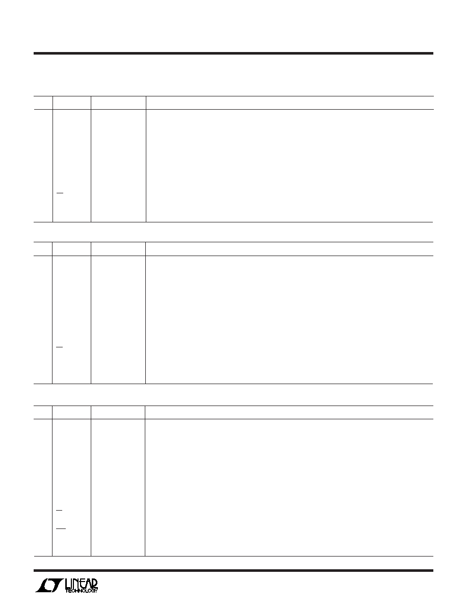
PI FU CTIO S
U
UU
#
PIN
FUNCTION
DESCRIPTION
1 – 6
CH0 – CH5
Analog Inputs
The analog inputs must be free of noise with respect to AGND.
7
COM
Common
The common pin defines the zero reference point for all single ended inputs. It must be free of noise and is
usually tied to the analog ground plane.
8
DGND
Digital Ground
This is the ground for the internal logic. Tie to the ground plane.
9V
–
Negative Supply
Tie V
– to most negative potential in the circuit (Ground in single supply applications).
10
AGND
Analog Ground
AGND should be tied directly to the analog ground plane.
11
VREF
Ref. Input
The reference inputs must be kept free of noise with respect to AGND.
12
DIN
Data Input
The A/D configuration word is shifted into this input.
13
DOUT
Digital Data Output The A/D conversion result is shifted out of this output.
14
CS
Chip Select Input
A logic low on this input enables data transfer.
15
CLK
Clock
This clock synchronizes the serial data transfer and controls A/D conversion rate.
16
VCC
Positive supply
This supply must be kept free of noise and ripple by bypassing directly to the analog ground plane.
LTC1293
#
PIN
FUNCTION
DESCRIPTION
1 –8
CH0 – CH7
Analog Inputs
The analog inputs must be free of noise with respect to AGND.
9
COM
Common
The common pin defines the zero reference point for all single ended inputs. It must be free of noise and is
usually tied to the analog ground plane.
10
DGND
Digital Ground
This is the ground for the internal logic. Tie to the ground plane.
11
V
–
Negative Supply
Tie V
– to most negative potential in the circuit (Ground in single supply applications).
12
AGND
Analog Ground
AGND should be tied directly to the analog ground plane.
13, 14 REF
–, REF+ Ref. Inputs
The reference inputs must be kept free of noise with respect to AGND. The A/D sees a reference voltage equal
to the difference between REF
+ and REF–.
15
DIN
Data Input
The A/D configuration word is shifted into this input.
16
DOUT
Digital Data Output The A/D conversion result is shifted out of this output.
17
CS
Chip Select Input
A logic low on this input enables data transfer.
18
CLK
Clock
This clock synchronizes the serial data transfer and controls A/D converion rate.
19, 20 AVCC, DVCC
Positive Supplies
These supplies must be kept free of noise and ripple by bypassing directly to the analog ground plane. AVCC
and DVCC must be tied together.
LTC1294
#
PIN
FUNCTION
DESCRIPTION
1 –8
CH0 – CH7
Analog Inputs
The analog inputs must be free of noise with respect to AGND.
9
COM
Common
The common pin defines the zero reference point for all single ended inputs. It must be free of noise and is
usually tied to the analog ground plane.
10
DGND
Digital Ground
This is the ground for the internal logic. Tie to the ground plane.
11
V
–
Negative Supply
Tie V
– to most negative potential in the circuit (Ground in single supply applications).
12
AGND
Analog Ground
AGND should be tied directly to the analog ground plane.
13, 14 REF
–, REF+ Ref. Inputs
The reference inputs must be kept free of noise with respect to AGND. The A/D sees a reference voltage equal
to the difference between REF
+ and REF–.
15
DIN
Data Input
The A/D configuration word is shifted into this input.
16
DOUT
Digital Data Output The A/D conversion result is shifted out of this output.
17
CS
Chip Select Input
A logic low on this input enables data transfer.
18
CLK
Clock
This clock synchronizes the serial data transfer and controls A/D conversion rate.
19
SSO
System Shutdown
System Shutdown Output pin will go low when power shutdown is requested.
Output
20
VCC
Positive Supply
This supply must be kept free of noise and ripple by bypassing directly to the analog ground plane.
LTC1296
相关PDF资料 |
PDF描述 |
|---|---|
| AD7890ARZ-4REEL | IC DAS 12BIT 8CH 24-SOIC |
| LTC1093CSW#TRPBF | IC DATA ACQ SYS 10BIT 6CH 16SOIC |
| LTC1093CSW#TR | IC DATA ACQ SYS 10BIT 6CH 16SOIC |
| LTC1093CSW#PBF | IC DATA ACQ SYS 10BIT 6CH 16SOIC |
| LTC1093CSW | IC DATA ACQ SYS 10BIT 6CH 16SOIC |
相关代理商/技术参数 |
参数描述 |
|---|---|
| LTC1296BIN | 功能描述:IC DATA ACQ SYSTEM 12BIT 20-DIP RoHS:否 类别:集成电路 (IC) >> 数据采集 - ADCs/DAC - 专用型 系列:- 产品培训模块:Lead (SnPb) Finish for COTS Obsolescence Mitigation Program 标准包装:50 系列:- 类型:数据采集系统(DAS) 分辨率(位):16 b 采样率(每秒):21.94k 数据接口:MICROWIRE?,QSPI?,串行,SPI? 电压电源:模拟和数字 电源电压:1.8 V ~ 3.6 V 工作温度:-40°C ~ 85°C 安装类型:表面贴装 封装/外壳:40-WFQFN 裸露焊盘 供应商设备封装:40-TQFN-EP(6x6) 包装:托盘 |
| LTC1296BIN#PBF | 功能描述:IC DATA ACQ SYSTEM 12BIT 20-DIP RoHS:是 类别:集成电路 (IC) >> 数据采集 - ADCs/DAC - 专用型 系列:- 产品培训模块:Lead (SnPb) Finish for COTS Obsolescence Mitigation Program 标准包装:50 系列:- 类型:数据采集系统(DAS) 分辨率(位):16 b 采样率(每秒):21.94k 数据接口:MICROWIRE?,QSPI?,串行,SPI? 电压电源:模拟和数字 电源电压:1.8 V ~ 3.6 V 工作温度:-40°C ~ 85°C 安装类型:表面贴装 封装/外壳:40-WFQFN 裸露焊盘 供应商设备封装:40-TQFN-EP(6x6) 包装:托盘 |
| LTC1296BISW | 功能描述:IC DATA ACQ SYSTEM 12BIT 20-SOIC RoHS:否 类别:集成电路 (IC) >> 数据采集 - ADCs/DAC - 专用型 系列:- 产品培训模块:Lead (SnPb) Finish for COTS Obsolescence Mitigation Program 标准包装:50 系列:- 类型:数据采集系统(DAS) 分辨率(位):16 b 采样率(每秒):21.94k 数据接口:MICROWIRE?,QSPI?,串行,SPI? 电压电源:模拟和数字 电源电压:1.8 V ~ 3.6 V 工作温度:-40°C ~ 85°C 安装类型:表面贴装 封装/外壳:40-WFQFN 裸露焊盘 供应商设备封装:40-TQFN-EP(6x6) 包装:托盘 |
| LTC1296BISW#PBF | 功能描述:IC DATA ACQ SYSTEM 12BIT 20-SOIC RoHS:是 类别:集成电路 (IC) >> 数据采集 - ADCs/DAC - 专用型 系列:- 产品培训模块:Lead (SnPb) Finish for COTS Obsolescence Mitigation Program 标准包装:50 系列:- 类型:数据采集系统(DAS) 分辨率(位):16 b 采样率(每秒):21.94k 数据接口:MICROWIRE?,QSPI?,串行,SPI? 电压电源:模拟和数字 电源电压:1.8 V ~ 3.6 V 工作温度:-40°C ~ 85°C 安装类型:表面贴装 封装/外壳:40-WFQFN 裸露焊盘 供应商设备封装:40-TQFN-EP(6x6) 包装:托盘 |
| LTC1296BISW#TR | 功能描述:IC DATA ACQ SYS 12BIT 5V 20SOIC RoHS:否 类别:集成电路 (IC) >> 数据采集 - ADCs/DAC - 专用型 系列:- 产品培训模块:Lead (SnPb) Finish for COTS Obsolescence Mitigation Program 标准包装:50 系列:- 类型:数据采集系统(DAS) 分辨率(位):16 b 采样率(每秒):21.94k 数据接口:MICROWIRE?,QSPI?,串行,SPI? 电压电源:模拟和数字 电源电压:1.8 V ~ 3.6 V 工作温度:-40°C ~ 85°C 安装类型:表面贴装 封装/外壳:40-WFQFN 裸露焊盘 供应商设备封装:40-TQFN-EP(6x6) 包装:托盘 |
发布紧急采购,3分钟左右您将得到回复。