- 您现在的位置:买卖IC网 > PDF目录9519 > LTC1296DCSW#PBF (Linear Technology)IC DATA ACQ SYSTEM 12BIT 20-SOIC PDF资料下载
参数资料
| 型号: | LTC1296DCSW#PBF |
| 厂商: | Linear Technology |
| 文件页数: | 14/28页 |
| 文件大小: | 0K |
| 描述: | IC DATA ACQ SYSTEM 12BIT 20-SOIC |
| 标准包装: | 38 |
| 类型: | 数据采集系统(DAS),ADC |
| 分辨率(位): | 12 b |
| 采样率(每秒): | 46.5k |
| 数据接口: | 串行,并联 |
| 电压电源: | 双 ± |
| 电源电压: | ±5V,5V |
| 工作温度: | 0°C ~ 70°C |
| 安装类型: | 表面贴装 |
| 封装/外壳: | 20-SOIC(0.295",7.50mm 宽) |
| 供应商设备封装: | 20-SOIC |
| 包装: | 管件 |
| 产品目录页面: | 1346 (CN2011-ZH PDF) |
第1页第2页第3页第4页第5页第6页第7页第8页第9页第10页第11页第12页第13页当前第14页第15页第16页第17页第18页第19页第20页第21页第22页第23页第24页第25页第26页第27页第28页
21
LTC1293/LTC1294/LTC1296
129346fs
Usually VERROR will not be significant. For a 60Hz signal
on the “–” input to generate a 0.25LSB error (300
V) with
the converter running at CLK = 1MHz, its peak value would
have to be 66mV. Rearranging the above equation the
maximum sinusoidal signal that can be digitized to a given
accuracy is given as:
For 0.25LSB error (300
V) the maximum input sinusoid
with a 5V peak amplitude that can be digitized is 0.8Hz.
Unused inputs should be tied to the ground plane.
Reference Input
The voltage on the reference input of the LTC1293/4/6
determines the voltage span of the A/D converter. The
reference input has transient capacitive switching cur-
rents due to the switched capacitor conversion technique
(see Figure 12). During each bit test of the conversion
(every CLK cycle) a capacitive current spike will be gener-
ated on the reference pin by the A/D. These current spikes
settle quickly and do not cause a problem. If slow settling
circuitry is used to drive the reference input, take care to
insure that transients caused by these current spikes settle
completely during each bit test of the conversion.
U
S
A
O
PPLICATI
WU
U
I FOR ATIO
Figure 13 and 14 show examples of both adequate and
poor settling. Using a slower CLK will allow more time for
the reference to settle. Even at the maximum CLK rate of
1MHz most references and op amps can be made to settle
within the 1
s bit time. For example the LT1027 will settle
adequately or with a 10
F bypass capacitor at VREF the
LT1021 also can be used.
VERTICAL:
0.5mV/DIV
VERTICAL:
0.5mV/DIV
Figure 14. Poor Reference Settling Can Cause A/D Errors
HORIZONTAL: 1
s/DIV
HORIZONTAL: 1
s/DIV
Figure 13. Adequate Reference Settling (LT1027)
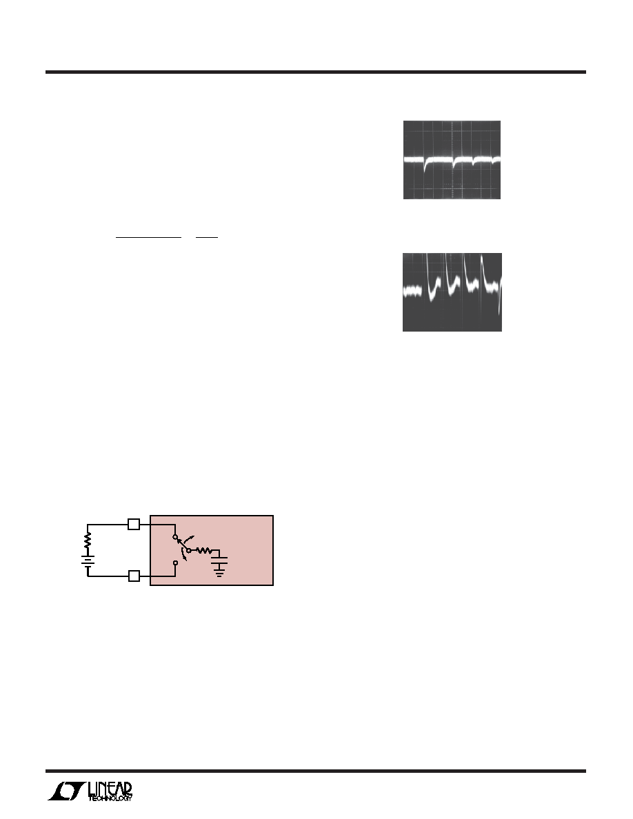
Figure 12. Reference Input Equivalent Circuit
RON
8pF – 40pF
LTC1293/4/6
REF+
ROUT
VREF
EVERY CLK CYCLE
14
13
REF–
LTC 1293 F12
Reduced Reference Operation
The effective resolution of the LTC1293/4/6 can be in-
creased by reducing the input span of the converter. The
LTC1293/4/6 exhibits good linearity over a range of refer-
ence voltages (see typical performance characteristics
curves of Change in Linearity vs Reference Voltage and
Change in Gain Error vs Reference Voltage). Care must be
taken when operating at low values of VREF because of the
reduced LSB step size and the resulting higher accuracy
requirement placed on the converter. Offset and Noise are
factors that must be considered when operating at low
VREF values. For the LTC1293 REF– has been tied to the
AGND pin. Any voltage drop from the AGND pin to the
ground plane will cause a gain error.
Offset with Reduced VREF
The offset of the LTC1293/4/6 has a larger effect on the
output code when the A/D is operated with a reduced
reference voltage. The offset (which is typically a fixed
voltage) becomes a larger fraction of an LSB as the size of
the LSB is reduced. The typical performance characteris-
tic curve of Unadjusted Offset Error vs Reference Voltage
shows how offset in LSB’s is related to reference voltage
for a typical value of VOS. For example a VOS of 0.1mV,
which is 0.1LSB with a 5V reference becomes 0.4LSB with
f
V
f
MAX
ERROR MAX
PEAK
CLK
(–)
()
=
π
2
12
相关PDF资料 |
PDF描述 |
|---|---|
| LTC6992IS6-2#TRMPBF | IC OSC SILICON 1MHZ TSOT23-6 |
| D38999/20MJ19SC | CONN RCPT 19POS WALL MNT W/SCKT |
| LTC1290DCN#PBF | IC DATA ACQ SYS 12BIT 20-DIP |
| MS27466T17A6P | CONN RCPT 6POS WALL MT W/PINS |
| MS27505E25F2SD | CONN RCPT 100POS BOX MNT W/SCKT |
相关代理商/技术参数 |
参数描述 |
|---|---|
| LTC1296DIN | 功能描述:IC DATA ACQ SYSTEM 12BIT 20-DIP RoHS:否 类别:集成电路 (IC) >> 数据采集 - ADCs/DAC - 专用型 系列:- 产品培训模块:Lead (SnPb) Finish for COTS Obsolescence Mitigation Program 标准包装:50 系列:- 类型:数据采集系统(DAS) 分辨率(位):16 b 采样率(每秒):21.94k 数据接口:MICROWIRE?,QSPI?,串行,SPI? 电压电源:模拟和数字 电源电压:1.8 V ~ 3.6 V 工作温度:-40°C ~ 85°C 安装类型:表面贴装 封装/外壳:40-WFQFN 裸露焊盘 供应商设备封装:40-TQFN-EP(6x6) 包装:托盘 |
| LTC1296DIN#PBF | 功能描述:IC DATA ACQ SYSTEM 12BIT 20-DIP RoHS:是 类别:集成电路 (IC) >> 数据采集 - ADCs/DAC - 专用型 系列:- 产品培训模块:Lead (SnPb) Finish for COTS Obsolescence Mitigation Program 标准包装:50 系列:- 类型:数据采集系统(DAS) 分辨率(位):16 b 采样率(每秒):21.94k 数据接口:MICROWIRE?,QSPI?,串行,SPI? 电压电源:模拟和数字 电源电压:1.8 V ~ 3.6 V 工作温度:-40°C ~ 85°C 安装类型:表面贴装 封装/外壳:40-WFQFN 裸露焊盘 供应商设备封装:40-TQFN-EP(6x6) 包装:托盘 |
| LTC1296DISW | 功能描述:IC DATA ACQ SYSTEM 12BIT 20-SOIC RoHS:否 类别:集成电路 (IC) >> 数据采集 - ADCs/DAC - 专用型 系列:- 产品培训模块:Lead (SnPb) Finish for COTS Obsolescence Mitigation Program 标准包装:50 系列:- 类型:数据采集系统(DAS) 分辨率(位):16 b 采样率(每秒):21.94k 数据接口:MICROWIRE?,QSPI?,串行,SPI? 电压电源:模拟和数字 电源电压:1.8 V ~ 3.6 V 工作温度:-40°C ~ 85°C 安装类型:表面贴装 封装/外壳:40-WFQFN 裸露焊盘 供应商设备封装:40-TQFN-EP(6x6) 包装:托盘 |
| LTC1296DISW#PBF | 功能描述:IC DATA ACQ SYSTEM 12BIT 20-SOIC RoHS:是 类别:集成电路 (IC) >> 数据采集 - ADCs/DAC - 专用型 系列:- 产品培训模块:Lead (SnPb) Finish for COTS Obsolescence Mitigation Program 标准包装:50 系列:- 类型:数据采集系统(DAS) 分辨率(位):16 b 采样率(每秒):21.94k 数据接口:MICROWIRE?,QSPI?,串行,SPI? 电压电源:模拟和数字 电源电压:1.8 V ~ 3.6 V 工作温度:-40°C ~ 85°C 安装类型:表面贴装 封装/外壳:40-WFQFN 裸露焊盘 供应商设备封装:40-TQFN-EP(6x6) 包装:托盘 |
| LTC1296DISW#TR | 功能描述:IC DATA ACQ SYS 12BIT 5V 20SOIC RoHS:否 类别:集成电路 (IC) >> 数据采集 - ADCs/DAC - 专用型 系列:- 产品培训模块:Lead (SnPb) Finish for COTS Obsolescence Mitigation Program 标准包装:50 系列:- 类型:数据采集系统(DAS) 分辨率(位):16 b 采样率(每秒):21.94k 数据接口:MICROWIRE?,QSPI?,串行,SPI? 电压电源:模拟和数字 电源电压:1.8 V ~ 3.6 V 工作温度:-40°C ~ 85°C 安装类型:表面贴装 封装/外壳:40-WFQFN 裸露焊盘 供应商设备封装:40-TQFN-EP(6x6) 包装:托盘 |
发布紧急采购,3分钟左右您将得到回复。