参数资料
| 型号: | LTC1297CCN8 |
| 厂商: | Linear Technology |
| 文件页数: | 13/24页 |
| 文件大小: | 0K |
| 描述: | IC DATA ACQ SYSTEM 12BIT 8-DIP |
| 标准包装: | 50 |
| 类型: | 数据采集系统(DAS) |
| 分辨率(位): | 12 b |
| 采样率(每秒): | 60k |
| 数据接口: | 串行,并联 |
| 电压电源: | 单电源 |
| 电源电压: | 5V |
| 工作温度: | 0°C ~ 70°C |
| 安装类型: | 通孔 |
| 封装/外壳: | 8-DIP(0.300",7.62mm) |
| 供应商设备封装: | 8-PDIP |
| 包装: | 管件 |
20
LTC1292/LTC1297
12927fb
U
S
A
O
PPLICATI
WU
U
I FOR ATIO
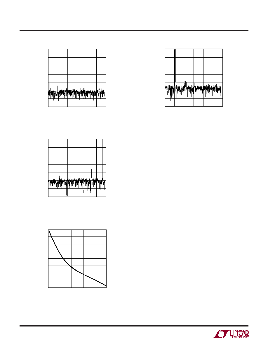
Figure 20a. fIN = 1kHz, fS = 58.8kHz, SNR = 73.0dB
Figure 20b. fIN = 28kHz, fS = 58.8kHz, SNR = 61.5dB
Figure 21. LTC1292 ENOB vs Input Frequency
Figure 22. fIN1 = 5.1kHz, fIN2 = 5.6kHz, fS = 58.8kHz
Overvoltage Protection
Applying signals to the LTC1292/LTC1297’s analog
inputs that exceed the positive supply or that go below
ground will degrade the accuracy of the A/D and possi-
bly damage the devices. For example this condition
would occur if a signal is applied to the analog inputs
before power is applied to the LTC1292/LTC1297. An-
other example is the input source is operating from
different supplies of larger value than the LTC1292/
LTC1297. These conditions should be prevented either
with proper supply sequencing or by use of external
circuitry to clamp or current limit the input source.
There are two ways to protect the inputs. In Figure 23
diode clamps from the inputs to VCC and GND are used.
The second method is to put resistors in series with the
analog inputs for current limiting. Limit the current to
15mA per channel. The +IN input can accept a resistor
value of 1k but the –IN input cannot accept more than
250
when clocked at its maximum clock frequency of
1MHz. If the LTC1292/LTC1297 are clocked at the
maximum clock frequency and 250
is not enough to
current limit the input source, then the clamp diodes are
recommended (Figures 24a and 24b). The reason for
the limit on the resistor value is that the MSB bit test is
affected by the value of the resistor placed at the –IN
input (see discussion on Analog Inputs and the typical
performance characteristics Maximum CLK Frequency
vs Source Resistance).
FREQUENCY (kHz)
0
–60
–40
–20
15
25
LTC1292/7 F20a
–80
–100
510
20
30
–120
–140
MAGNITUDE
(dB)
0
FREQUENCY (kHz)
0
–60
–40
–20
15
25
LTC1292/7 F22
–80
–100
510
20
30
–120
–140
MAGNITUDE
(dB)
0
FREQUENCY (kHz)
0
–60
–40
–20
15
25
LTC1292/7 F20b
–80
–100
510
20
30
–120
–140
MAGNITUDE
(dB)
0
FREQUENCY (kHz)
0
EFFECTIVE
NUMBER
OF
BITS
9.5
10.0
10.5
60
100
LT1292/7 F21
9.0
8.5
8.0
20
40
80
11.0
11.5
12.0
fS = 58.8kHz
相关PDF资料 |
PDF描述 |
|---|---|
| VI-B1J-IU-F4 | CONVERTER MOD DC/DC 36V 200W |
| VI-B1J-IU-F3 | CONVERTER MOD DC/DC 36V 200W |
| AD7890BRZ-10REEL | IC DAS 12BIT 8CH 24-SOIC |
| VI-B1J-IU-F2 | CONVERTER MOD DC/DC 36V 200W |
| AD7890BRZ-2REEL | IC DAS 12BIT 8CH 24-SOIC |
相关代理商/技术参数 |
参数描述 |
|---|---|
| LTC1297CCN8#PBF | 功能描述:IC DATA ACQ SYSTEM 12BIT 8-DIP RoHS:是 类别:集成电路 (IC) >> 数据采集 - ADCs/DAC - 专用型 系列:- 产品培训模块:Lead (SnPb) Finish for COTS Obsolescence Mitigation Program 标准包装:50 系列:- 类型:数据采集系统(DAS) 分辨率(位):16 b 采样率(每秒):21.94k 数据接口:MICROWIRE?,QSPI?,串行,SPI? 电压电源:模拟和数字 电源电压:1.8 V ~ 3.6 V 工作温度:-40°C ~ 85°C 安装类型:表面贴装 封装/外壳:40-WFQFN 裸露焊盘 供应商设备封装:40-TQFN-EP(6x6) 包装:托盘 |
| LTC1297CCN8PBF | 制造商:Linear Technology 功能描述:LTC1297CCN8PBF |
| LTC1297DCJ8 | 制造商:Linear Technology 功能描述:ADC Single SAR 50ksps 12-bit Serial 8-Pin CDIP |
| LTC1297DCN8 | 功能描述:IC DATA ACQ SYSTEM 12BIT 8-DIP RoHS:否 类别:集成电路 (IC) >> 数据采集 - ADCs/DAC - 专用型 系列:- 产品培训模块:Lead (SnPb) Finish for COTS Obsolescence Mitigation Program 标准包装:50 系列:- 类型:数据采集系统(DAS) 分辨率(位):16 b 采样率(每秒):21.94k 数据接口:MICROWIRE?,QSPI?,串行,SPI? 电压电源:模拟和数字 电源电压:1.8 V ~ 3.6 V 工作温度:-40°C ~ 85°C 安装类型:表面贴装 封装/外壳:40-WFQFN 裸露焊盘 供应商设备封装:40-TQFN-EP(6x6) 包装:托盘 |
| LTC1297DCN8#PBF | 功能描述:IC DATA ACQ SYSTEM 12BIT 8-DIP RoHS:是 类别:集成电路 (IC) >> 数据采集 - ADCs/DAC - 专用型 系列:- 产品培训模块:Lead (SnPb) Finish for COTS Obsolescence Mitigation Program 标准包装:50 系列:- 类型:数据采集系统(DAS) 分辨率(位):16 b 采样率(每秒):21.94k 数据接口:MICROWIRE?,QSPI?,串行,SPI? 电压电源:模拟和数字 电源电压:1.8 V ~ 3.6 V 工作温度:-40°C ~ 85°C 安装类型:表面贴装 封装/外壳:40-WFQFN 裸露焊盘 供应商设备封装:40-TQFN-EP(6x6) 包装:托盘 |
发布紧急采购,3分钟左右您将得到回复。