- 您现在的位置:买卖IC网 > PDF目录10292 > LTC1298IN8#PBF (Linear Technology)IC A/D CONV SAMPLING 12BIT 8-DIP PDF资料下载
参数资料
| 型号: | LTC1298IN8#PBF |
| 厂商: | Linear Technology |
| 文件页数: | 22/24页 |
| 文件大小: | 0K |
| 描述: | IC A/D CONV SAMPLING 12BIT 8-DIP |
| 标准包装: | 50 |
| 位数: | 12 |
| 采样率(每秒): | 11.1k |
| 数据接口: | MICROWIRE?,串行,SPI? |
| 转换器数目: | 1 |
| 功率耗散(最大): | 1.8mW |
| 电压电源: | 单电源 |
| 工作温度: | -40°C ~ 85°C |
| 安装类型: | 通孔 |
| 封装/外壳: | 8-DIP(0.300",7.62mm) |
| 供应商设备封装: | 8-PDIP |
| 包装: | 管件 |
| 输入数目和类型: | 2 个单端,单极 |
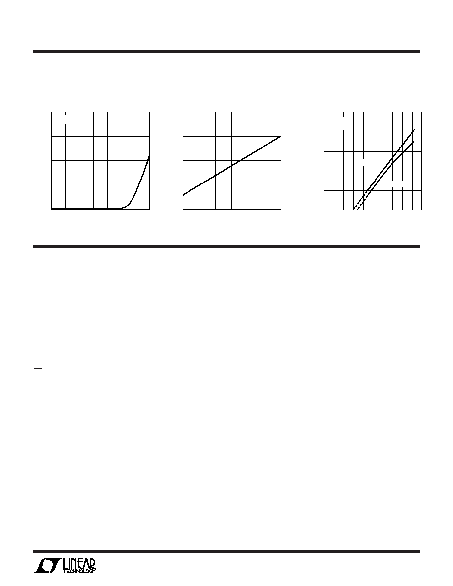
7
LTC1286/LTC1298
TYPICAL PERFORMANCE CHARACTERISTICS
U
W
TEMPERATURE (°C)
–55
CLOCK
FREQUENCY
(kHz)
100
150
25
45
65
85
LT1286/98 G14
50
0
–35
–15
5
200
VCC = VREF = 5V
SUPPLY VOLTAGE (V)
3
1
DIGITAL
LOGIC
THRESHOLD
VOLTAGE
(V)
2
3
45
6
7
LTC 1286/98 G17
89
TA = 25°C
TEMPERATURE (°C)
–60
LEAKAGE
CURRENT
(nA)
1000
100
10
1
0.1
0.01
100
1196/98 G19
–20
20
60
140
–40
0
40
80
120
VCC = 5V
VREF = 5V
ON CHANNEL
OFF CHANNEL
Input Channel Leakage Current
vs Temperature
Digital Input Logic Threshold
vs Supply Voltage
Minimum Clock Frequency
for 0.1 LSB Error vs Temperature
PIN FUNCTIONS
UU
U
LTC1286
VREF (Pin 1): Reference Input. The reference input defines
the span of the A/D converter.
IN+ (Pin 2): Positive Analog Input.
IN – (Pin 3): Negative Analog Input.
GND (Pin 4): Analog Ground. GND should be tied directly
to an analog ground plane.
CS/SHDN (Pin 5): Chip Select Input. A logic low on this
input enables the LTC1286. A logic high on this input
disables and powers down the LTC1286.
DOUT (Pin 6): Digital Data Output. The A/D conversion
result is shifted out of this output.
CLK (Pin 7): Shift Clock. This clock synchronizes the serial
data transfer and determines conversion speed.
VCC (Pin 8): Power Supply Voltage. This pin provides
power to the A/D converter. It must be kept free of noise
and ripple by bypassing directly to the analog ground
plane.
LTC1298
CS/SHDN (Pin 1): Chip Select Input. A logic low on this
input enables the LTC1298. A logic high on this input
disables and powers down the LTC1298.
CH0 (Pin 2): Analog Input.
CH1 (Pin 3): Analog Input.
GND (Pin 4): Analog Ground. GND should be tied directly
to an analog ground plane.
DIN (Pin 5): Digital Data Input. The multiplexer address is
shifted into this input.
DOUT (Pin 6): Digital Data Output. The A/D conversion
result is shifted out of this output.
CLK (Pin 7): Shift Clock. This clock synchronizes the
serial data transfer and determines conversion speed.
VCC/VREF (Pin 8): Power Supply and Reference Voltage.
This pin provides power and defines the span of the A/D
converter. It must be kept free of noise and ripple by
bypassing directly to the analog ground plane.
相关PDF资料 |
PDF描述 |
|---|---|
| VE-232-MY | CONVERTER MOD DC/DC 15V 50W |
| D38999/24MF11PNLC | CONN HSG RCPT 11POS JAM NUT PINS |
| D38999/26FG75AA | CONN HSG PLUG 4POS STRGHT PINS |
| D38999/20FC98PA | CONN RCPT 10POS WALL MNT W/PINS |
| LTC1298IN8 | IC A/D CONV SAMPLING 12BIT 8-DIP |
相关代理商/技术参数 |
参数描述 |
|---|---|
| LTC1298IS8 | 功能描述:IC A/D CONV SAMPLING 12BIT 8SOIC RoHS:否 类别:集成电路 (IC) >> 数据采集 - 模数转换器 系列:- 标准包装:1,000 系列:- 位数:16 采样率(每秒):45k 数据接口:串行 转换器数目:2 功率耗散(最大):315mW 电压电源:模拟和数字 工作温度:0°C ~ 70°C 安装类型:表面贴装 封装/外壳:28-SOIC(0.295",7.50mm 宽) 供应商设备封装:28-SOIC W 包装:带卷 (TR) 输入数目和类型:2 个单端,单极 |
| LTC1298IS8#PBF | 功能描述:IC A/D CONV SAMPLING 12BIT 8SOIC RoHS:是 类别:集成电路 (IC) >> 数据采集 - 模数转换器 系列:- 其它有关文件:TSA1204 View All Specifications 标准包装:1 系列:- 位数:12 采样率(每秒):20M 数据接口:并联 转换器数目:2 功率耗散(最大):155mW 电压电源:模拟和数字 工作温度:-40°C ~ 85°C 安装类型:表面贴装 封装/外壳:48-TQFP 供应商设备封装:48-TQFP(7x7) 包装:Digi-Reel® 输入数目和类型:4 个单端,单极;2 个差分,单极 产品目录页面:1156 (CN2011-ZH PDF) 其它名称:497-5435-6 |
| LTC1298IS8#PBF | 制造商:Linear Technology 功能描述:IC ADC 12BIT 11.1KSPS SOIC-8 制造商:Linear Technology 功能描述:IC, ADC, 12BIT, 11.1KSPS, SOIC-8 |
| LTC1298IS8#TR | 功能描述:IC ADC 12BIT SAMPL MCRPWR 8SOIC RoHS:否 类别:集成电路 (IC) >> 数据采集 - 模数转换器 系列:- 标准包装:1,000 系列:- 位数:16 采样率(每秒):45k 数据接口:串行 转换器数目:2 功率耗散(最大):315mW 电压电源:模拟和数字 工作温度:0°C ~ 70°C 安装类型:表面贴装 封装/外壳:28-SOIC(0.295",7.50mm 宽) 供应商设备封装:28-SOIC W 包装:带卷 (TR) 输入数目和类型:2 个单端,单极 |
| LTC1298IS8#TRPBF | 功能描述:IC A/D CONV SAMPLING 12BIT 8SOIC RoHS:是 类别:集成电路 (IC) >> 数据采集 - 模数转换器 系列:- 标准包装:1,000 系列:- 位数:16 采样率(每秒):45k 数据接口:串行 转换器数目:2 功率耗散(最大):315mW 电压电源:模拟和数字 工作温度:0°C ~ 70°C 安装类型:表面贴装 封装/外壳:28-SOIC(0.295",7.50mm 宽) 供应商设备封装:28-SOIC W 包装:带卷 (TR) 输入数目和类型:2 个单端,单极 |
发布紧急采购,3分钟左右您将得到回复。