- 您现在的位置:买卖IC网 > PDF目录10541 > LTC1298IS8#PBF (Linear Technology)IC A/D CONV SAMPLING 12BIT 8SOIC PDF资料下载
参数资料
| 型号: | LTC1298IS8#PBF |
| 厂商: | Linear Technology |
| 文件页数: | 4/24页 |
| 文件大小: | 0K |
| 描述: | IC A/D CONV SAMPLING 12BIT 8SOIC |
| 标准包装: | 100 |
| 位数: | 12 |
| 采样率(每秒): | 11.1k |
| 数据接口: | MICROWIRE?,串行,SPI? |
| 转换器数目: | 1 |
| 功率耗散(最大): | 1.8mW |
| 电压电源: | 单电源 |
| 工作温度: | -40°C ~ 85°C |
| 安装类型: | 表面贴装 |
| 封装/外壳: | 8-SOIC(0.154",3.90mm 宽) |
| 供应商设备封装: | 8-SOIC |
| 包装: | 管件 |
| 输入数目和类型: | 2 个单端,单极 |
| 产品目录页面: | 1346 (CN2011-ZH PDF) |
12
LTC1286/LTC1298
Start Bit
The first “logical one” clocked into the DIN input after CS
goes low is the start bit. The start bit initiates the data
transfer. The LTC1298 will ignore all leading zeros which
precede this logical one. After the start bit is received, the
remaining bits of the input word will be clocked in. Further
inputs on the DIN pin are then ignored until the next CS
cycle.
Multiplexer (MUX) Address
The bits of the input word following the START bit assign
the MUX configuration for the requested conversion. For
a given channel selection, the converter will measure the
voltage between the two channels indicated by the + and
– signs in the selected row of the following tables. In
single-ended mode, all input channels are measured with
respect to GND.
APPLICATION INFORMATION
WU
U
Input Data Word
The LTC1286 requires no DIN word. It is permanently
configured to have a single differential input. The conver-
sion result appears on the DOUT line. The data format is
MSB first followed by the LSB sequence. This provides
easy interface to MSB or LSB first serial ports. For MSB
first data the CS signal can be taken high after B0 (see
Figure 1). The LTC1298 clocks data into the DIN input on
the rising edge of the clock. The input data words are
defined as follows:
MSBF bit is a logical zero, LSB first data will follow the
normal MSB first data on the DOUT line. (see Operating
Sequence)
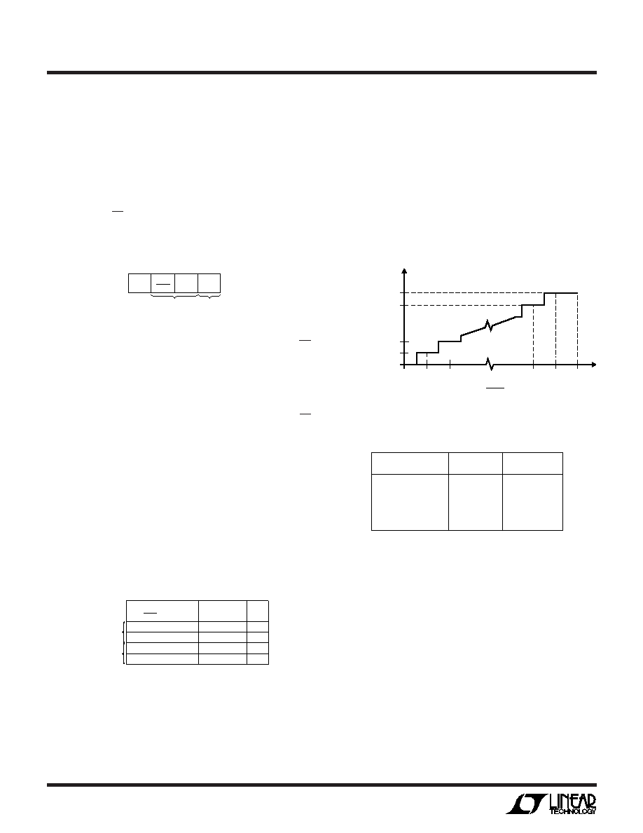
Transfer Curve
The LTC1286/LTC1298 are permanently configured for
unipolar only. The input span and code assignment for
this conversion type are shown in the following figures.
MSB First/LSB First (MSBF)
The output data of the LTC1298 is programmed for
MSB first or LSB first sequence using the MSBF bit.
When the MSBF bit is a logical one, data will appear on
the DOUT line in MSB first format. Logical zeros will be
filled in indefinitely following the last data bit. When the
Operation with DIN and DOUT Tied Together
The LTC1298 can be operated with DIN and DOUT tied
together. This eliminates one of the lines required to
communicate to the microprocessor (MPU). Data is trans-
mitted in both directions on a single wire. The processor
pin connected to this data line should be configurable as
either an input or an output. The LTC1298 will take control
of the data line and drive it low on the 4th falling CLK edge
after the start bit is received (see Figure 3). Therefore the
processor port line must be switched to an input before
this happens to avoid a conflict.
In the Typical Applications section, there is an example of
interfacing the LTC1298 with DINand DOUT tied together to
the Intel 8051 MPU.
OUTPUT CODE
1 1 1 1 1 1 1 1 1 1 1 1 1 1
1 1 1 1 1 1 1 1 1 1 1 1 1 0
0 0 0 0 0 0 0 0 0 0 0 0 0 1
0 0 0 0 0 0 0 0 0 0 0 0 0 0
INPUT VOLTAGE
VREF – 1LSB
VREF – 2LSB
1LSB
0V
INPUT VOLTAGE
(VREF = 5.000V)
4.99878V
4.99756V
0.00122V
0V
LTC1286/98 AI05
Transfer Curve
0V
1LSB
V
REF
–2LSB
VREF
4096
V
REF
–1LSB
V
REF
VIN
0 0 0 0 0 0 0 0 0 0 0 1
0 0 0 0 0 0 0 0 0 0 0 0
1 1 1 1 1 1 1 1 1 1 1 1
1 1 1 1 1 1 1 1 1 1 1 0
LTC1286/98 AI04
1LSB =
MUX ADDRESS
SGL/DIFF
1
0
ODD/SIGN
0
1
0
1
CHANNEL #
0
+
–
1
+
–
+
GND
–
SINGLE-ENDED
MUX MODE
DIFFERENTIAL
MUX MODE
LTC1096/8 AI03
SGL/
DIFF
ODD/
SIGN
MSBF
START
MUX
ADDRESS
MSB FIRST/
LSB FIRST
LTC1096/9 AI02
LTC1298 Channel Selection
Output Code
相关PDF资料 |
PDF描述 |
|---|---|
| MS3102A20-15PW | CONN RCPT 7POS BOX MNT W/PINS |
| AD7264BSTZ | IC ADC 14BIT 2CH 1MSPS 48LQFP |
| MS3102A22-18P | CONN RCPT 8POS BOX MNT W/PINS |
| VE-J53-MW-F2 | CONVERTER MOD DC/DC 24V 100W |
| LTC1594LIS#PBF | IC A/D CONV 12BIT SRL 4CH 16SOIC |
相关代理商/技术参数 |
参数描述 |
|---|---|
| LTC1314CS | 功能描述:IC PCMCIA SWITCHNG MATRIX 14SOIC RoHS:否 类别:集成电路 (IC) >> PMIC - 电源分配开关 系列:- 特色产品:XRP252 Switches 标准包装:1 系列:- 类型:高端开关 输出数:2 Rds(开):140 毫欧 内部开关:是 电流限制:1.15A 输入电压:1.75 V ~ 5.5 V 工作温度:-40°C ~ 85°C 安装类型:表面贴装 封装/外壳:10-WFDFN 裸露焊盘 供应商设备封装:10-TDFN(3x3) 包装:Digi-Reel® 其它名称:1016-1691-6 |
| LTC1314CS#PBF | 功能描述:IC PCMCIA SWITCHNG MATRIX 14SOIC RoHS:是 类别:集成电路 (IC) >> PMIC - 电源分配开关 系列:- 特色产品:XRP252 Switches 标准包装:1 系列:- 类型:高端开关 输出数:2 Rds(开):140 毫欧 内部开关:是 电流限制:1.15A 输入电压:1.75 V ~ 5.5 V 工作温度:-40°C ~ 85°C 安装类型:表面贴装 封装/外壳:10-WFDFN 裸露焊盘 供应商设备封装:10-TDFN(3x3) 包装:Digi-Reel® 其它名称:1016-1691-6 |
| LTC1314CS#TR | 功能描述:IC SW MATRIX PCMCIA SGL 14SOIC RoHS:否 类别:集成电路 (IC) >> PMIC - 电源分配开关 系列:- 特色产品:XRP252 Switches 标准包装:1 系列:- 类型:高端开关 输出数:2 Rds(开):140 毫欧 内部开关:是 电流限制:1.15A 输入电压:1.75 V ~ 5.5 V 工作温度:-40°C ~ 85°C 安装类型:表面贴装 封装/外壳:10-WFDFN 裸露焊盘 供应商设备封装:10-TDFN(3x3) 包装:Digi-Reel® 其它名称:1016-1691-6 |
| LTC1314CS#TRPBF | 功能描述:IC PCMCIA SWITCHNG MATRIX 14SOIC RoHS:是 类别:集成电路 (IC) >> PMIC - 电源分配开关 系列:- 特色产品:XRP252 Switches 标准包装:1 系列:- 类型:高端开关 输出数:2 Rds(开):140 毫欧 内部开关:是 电流限制:1.15A 输入电压:1.75 V ~ 5.5 V 工作温度:-40°C ~ 85°C 安装类型:表面贴装 封装/外壳:10-WFDFN 裸露焊盘 供应商设备封装:10-TDFN(3x3) 包装:Digi-Reel® 其它名称:1016-1691-6 |
| LTC1315CG#PBF | 功能描述:IC PCMCIA SWITCHNG MATRIX 24SSOP RoHS:是 类别:集成电路 (IC) >> PMIC - 电源分配开关 系列:- 标准包装:80 系列:- 类型:USB 开关 输出数:2 Rds(开):135 毫欧 内部开关:是 电流限制:1.5A 输入电压:2.7 V ~ 5.5 V 工作温度:-40°C ~ 85°C 安装类型:表面贴装 封装/外壳:8-TSSOP,8-MSOP(0.118",3.00mm 宽)裸露焊盘 供应商设备封装:8-MSOP-PowerPad 包装:管件 配用:TPS2066-1EVM-296-ND - TPS2066-1EVM-296 |
发布紧急采购,3分钟左右您将得到回复。