- 您现在的位置:买卖IC网 > PDF目录10283 > LTC1298IS8 (Linear Technology)IC A/D CONV SAMPLING 12BIT 8SOIC PDF资料下载
参数资料
| 型号: | LTC1298IS8 |
| 厂商: | Linear Technology |
| 文件页数: | 2/24页 |
| 文件大小: | 0K |
| 描述: | IC A/D CONV SAMPLING 12BIT 8SOIC |
| 标准包装: | 100 |
| 位数: | 12 |
| 采样率(每秒): | 11.1k |
| 数据接口: | MICROWIRE?,串行,SPI? |
| 转换器数目: | 1 |
| 功率耗散(最大): | 1.8mW |
| 电压电源: | 单电源 |
| 工作温度: | -40°C ~ 85°C |
| 安装类型: | 表面贴装 |
| 封装/外壳: | 8-SOIC(0.154",3.90mm 宽) |
| 供应商设备封装: | 8-SOIC |
| 包装: | 管件 |
| 输入数目和类型: | 2 个单端,单极 |
10
LTC1286/LTC1298
APPLICATION INFORMATION
WU
U
SERIAL INTERFACE
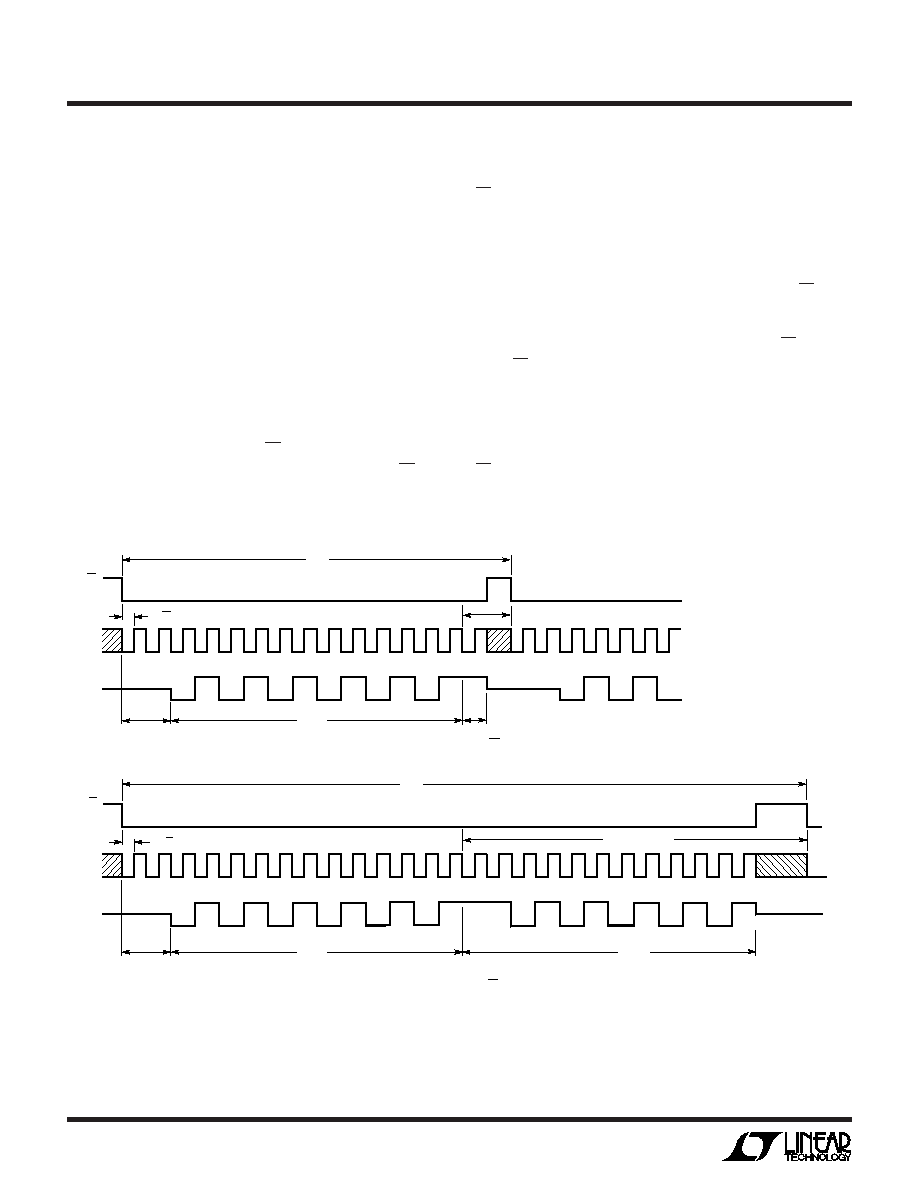
The 2-channel LTC1298 communicates with micropro-
cessors and other external circuitry via a synchronous,
half duplex, 4-wire serial interface. The single channel
LTC1286 uses a 3-wire interface (see Operating Sequence
in Figures 1 and 2).
Data Transfer
The CLK synchronizes the data transfer with each bit being
transmitted on the falling CLK edge and captured on the
rising CLK edge in both transmitting and receiving systems.
The LTC1286 does not require a configuration input word
and has no DIN pin. A falling CS initiates data transfer as
shown in the LTC1286 operating sequence. After CS falls
the second CLK pulse enables DOUT. After one null bit the
A/D conversion result is output on the DOUT line. Bringing
CS high resets the LTC1286 for the next data exchange.
The LTC1298 first receives input data and then transmits
back the A/D conversion result (half duplex). Because of
the half duplex operation, DIN and DOUT may be tied
together allowing transmission over just 3 wires: CS, CLK
and DATA (DIN/DOUT).
Data transfer is initiated by a falling chip select (CS) signal.
After CS falls the LTC1298 looks for a start bit. After the
start bit is received, the 3-bit input word is shifted into the
DIN input which configures the LTC1298 and starts the
conversion. After one null bit, the result of the conversion
is output on the DOUT line. At the end of the data exchange
CS should be brought high. This resets the LTC1298 in
preparation for the next data exchange.
CLK
CS
tCYC
B11
B5
B6
B7
B8
B9
B10
B11
HI-Z
DOUT
tCONV
tDATA
HI-Z
tsuCS
NULL
BIT
B4
B3
B2
B1
POWER
DOWN
POWER DOWN
B0*
NULL
BIT
B10
B9
B8
tSMPL
(MSB)
CLK
CS
tCYC
B11*
B5
B6
B7
B8
B9
B10
B11
HI-Z
DOUT
tCONV
tDATA
HI-Z
tsuCS
NULL
BIT
LTC1286/98 F01
B4
B3
B4
B5
B6
B7
B2
B1
B0
B1
B10
B9
B8
tSMPL
*AFTER COMPLETING THE DATA TRANSFER, IF FURTHER CLOCKS ARE APPLIED WITH CS LOW,
THE ADC WILL OUTPUT ZEROS INDEFINITELY.
*AFTER COMPLETING THE DATA TRANSFER, IF FURTHER CLOCKS ARE APPLIED WITH CS LOW,
THE ADC WILL OUTPUT LSB-FIRST DATA THEN FOLLOWED WITH ZEROS INDEFINITELY.
tDATA: DURING THIS TIME, THE BIAS CIRCUIT AND THE COMPARATOR POWER DOWN AND THE REFERENCE INPUT
BECOMES A HIGH IMPEDANCE NODE, LEAVING THE CLK RUNNING TO CLOCK OUT LSB-FIRST DATA OR ZEROES.
Figure 1. LTC1286 Operating Sequence
相关PDF资料 |
PDF描述 |
|---|---|
| D38999/20JJ4PALC | CONN HSG RCPT 56POS WALL MT PINS |
| VE-2NP-IU-S | CONVERTER MOD DC/DC 13.8V 200W |
| D38999/26FH53SNLC | CONN HSG PLUG 53POS STRGHT SCKT |
| D38999/26JE99PNLC | CONN HSG PLUG 23POS STRGHT PINS |
| VE-2NN-MY | CONVERTER MOD DC/DC 18.5V 50W |
相关代理商/技术参数 |
参数描述 |
|---|---|
| LTC1298IS8#PBF | 功能描述:IC A/D CONV SAMPLING 12BIT 8SOIC RoHS:是 类别:集成电路 (IC) >> 数据采集 - 模数转换器 系列:- 其它有关文件:TSA1204 View All Specifications 标准包装:1 系列:- 位数:12 采样率(每秒):20M 数据接口:并联 转换器数目:2 功率耗散(最大):155mW 电压电源:模拟和数字 工作温度:-40°C ~ 85°C 安装类型:表面贴装 封装/外壳:48-TQFP 供应商设备封装:48-TQFP(7x7) 包装:Digi-Reel® 输入数目和类型:4 个单端,单极;2 个差分,单极 产品目录页面:1156 (CN2011-ZH PDF) 其它名称:497-5435-6 |
| LTC1298IS8#PBF | 制造商:Linear Technology 功能描述:IC ADC 12BIT 11.1KSPS SOIC-8 制造商:Linear Technology 功能描述:IC, ADC, 12BIT, 11.1KSPS, SOIC-8 |
| LTC1298IS8#TR | 功能描述:IC ADC 12BIT SAMPL MCRPWR 8SOIC RoHS:否 类别:集成电路 (IC) >> 数据采集 - 模数转换器 系列:- 标准包装:1,000 系列:- 位数:16 采样率(每秒):45k 数据接口:串行 转换器数目:2 功率耗散(最大):315mW 电压电源:模拟和数字 工作温度:0°C ~ 70°C 安装类型:表面贴装 封装/外壳:28-SOIC(0.295",7.50mm 宽) 供应商设备封装:28-SOIC W 包装:带卷 (TR) 输入数目和类型:2 个单端,单极 |
| LTC1298IS8#TRPBF | 功能描述:IC A/D CONV SAMPLING 12BIT 8SOIC RoHS:是 类别:集成电路 (IC) >> 数据采集 - 模数转换器 系列:- 标准包装:1,000 系列:- 位数:16 采样率(每秒):45k 数据接口:串行 转换器数目:2 功率耗散(最大):315mW 电压电源:模拟和数字 工作温度:0°C ~ 70°C 安装类型:表面贴装 封装/外壳:28-SOIC(0.295",7.50mm 宽) 供应商设备封装:28-SOIC W 包装:带卷 (TR) 输入数目和类型:2 个单端,单极 |
| LTC1298IS8PBF | 制造商:Linear Technology 功能描述:12-Bit ADC uPower Sampling 2-Ch MUX SO8 |
发布紧急采购,3分钟左右您将得到回复。