- 您现在的位置:买卖IC网 > PDF目录10011 > LTC1350IG#PBF (Linear Technology)IC TXRX 3.3V EIA/TIA-562 28-SSOP PDF资料下载
参数资料
| 型号: | LTC1350IG#PBF |
| 厂商: | Linear Technology |
| 文件页数: | 5/8页 |
| 文件大小: | 0K |
| 描述: | IC TXRX 3.3V EIA/TIA-562 28-SSOP |
| 标准包装: | 47 |
| 类型: | 收发器 |
| 驱动器/接收器数: | 3/5 |
| 规程: | RS562 |
| 电源电压: | 3 V ~ 3.6 V |
| 安装类型: | 表面贴装 |
| 封装/外壳: | 28-SSOP(0.209",5.30mm 宽) |
| 供应商设备封装: | 28-SSOP |
| 包装: | 管件 |
| 产品目录页面: | 1354 (CN2011-ZH PDF) |
5
LTC1350
1350fa
UU
U
PI FU CTIO S
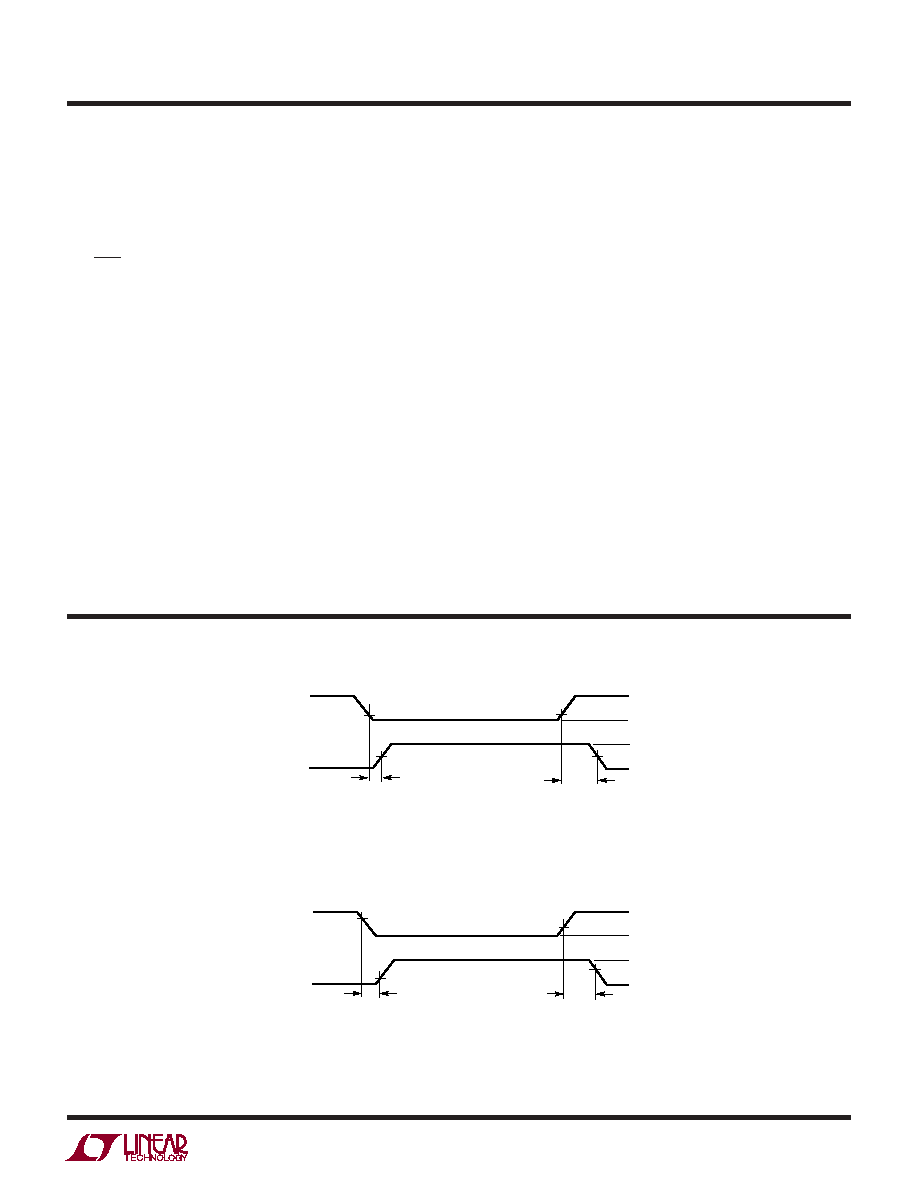
SWITCHI G TI E WAVEFOR S
UW
W
1.4V
0V
VCC
0V
V+
V–
0V
DR
INPUT
DR
OUTPUT
1.4V
tHLD
tLHD
LTC1350 F01
0.8V
VCC
0V
2.4V
RX
INPUT
RX
OUTPUT
1.3V
tHLR
1.7V
tLHR
LTC1350 F02
VCC
0V
Figure 2. Receiver Propagation Delay Timing
Figure 1. Driver Propagation Delay Timing
C1+, C1–, C2+, C2–: Commutating Capacitor Inputs. These
pins require two external capacitors (C = 0.1F): one from
C1+ to C1– and another from C2+ to C2 –. To maintain
charge pump efficiency, the capacitor’s effective series
resistance should be less than 20.
DR IN: EIA/TIA-562 Driver Input Pins. Inputs are TTL/
CMOS compatible. Inputs should not be allowed to float.
Tie unused inputs to VCC.
DR OUT: Driver Outputs at EIA/TIA-562 Voltage Levels.
Outputs are in a high impedance state when in the Shutdown
mode or VCC = 0V. The driver outputs are protected against
ESD to ±10kV for human body model discharges.
RX IN: Receiver Inputs. These pins can be forced to ±25V
without damage. The receiver inputs are protected against
ESD to ±10kV for human body model discharges. Each
receiver provides 0.4V of hysteresis for noise immunity.
RX OUT: Receiver Outputs with TTL/CMOS Voltage Levels.
Receiver 1, 2 and 3 outputs are in a high impedance state
when in Shutdown mode to allow data line sharing.
Receivers 4 and 5 are kept alive in Shutdown.
VCC: 3.3V Input Supply Pin. Supply current is typically
35A in the Shutdown mode. This pin should be decoupled
with a 0.1F ceramic capacitor.
GND: Ground Pin.
ON/OFF: TTL/CMOS Compatible Shutdown Pin. A logic
low puts the device in the Shutdown mode with receivers
4 and 5 kept alive and the supply current equal to 35A. All
driver and other receiver outputs are in high impedance
state. This pin cannot float.
V+: Positive Supply Output. V+ 2VCC – 1V. This pin
requires an external capacitor (C = 0.1F) for charge
storage. The capacitor may be tied to ground or VCC. With
multiple devices, the V + and V – pins may be paralleled into
common capacitors. For a large number of devices,
increasing the size of the shared common storage
capacitors is recommended to reduce ripple.
V–: Negative Supply Output. V – – (2VCC – 1.3V). This
pin requires an external capacitor (C = 0.1F) for charge
storage.
相关PDF资料 |
PDF描述 |
|---|---|
| VI-B3B-MX-B1 | CONVERTER MOD DC/DC 95V 75W |
| VE-B6P-IV-F1 | CONVERTER MOD DC/DC 13.8V 150W |
| IDT72V3631L15PF8 | IC SYNCFIFO 512X36 15NS 120-TQFP |
| VE-26B-IU-F1 | CONVERTER MOD DC/DC 95V 200W |
| LTC1345ISW#TR | IC TXRX V.35 SGL SUPPLY 28SOIC |
相关代理商/技术参数 |
参数描述 |
|---|---|
| LTC1350INW | 功能描述:IC TXRX 3.3V EIA/TIA-562 28-DIP RoHS:否 类别:集成电路 (IC) >> 接口 - 驱动器,接收器,收发器 系列:- 标准包装:27 系列:- 类型:收发器 驱动器/接收器数:3/3 规程:RS232,RS485 电源电压:4.75 V ~ 5.25 V 安装类型:表面贴装 封装/外壳:28-SOIC(0.295",7.50mm 宽) 供应商设备封装:28-SOIC 包装:管件 |
| LTC1350ISW | 功能描述:IC TXRX 3.3V EIA/TIA-562 28-SOIC RoHS:否 类别:集成电路 (IC) >> 接口 - 驱动器,接收器,收发器 系列:- 标准包装:27 系列:- 类型:收发器 驱动器/接收器数:3/3 规程:RS232,RS485 电源电压:4.75 V ~ 5.25 V 安装类型:表面贴装 封装/外壳:28-SOIC(0.295",7.50mm 宽) 供应商设备封装:28-SOIC 包装:管件 |
| LTC1350ISW#PBF | 功能描述:IC TXRX 3.3V EIA/TIA-562 28-SOIC RoHS:是 类别:集成电路 (IC) >> 接口 - 驱动器,接收器,收发器 系列:- 标准包装:1,140 系列:AU 类型:收发器 驱动器/接收器数:1/1 规程:CAN 电源电压:5.3 V ~ 27 V 安装类型:表面贴装 封装/外壳:14-SOIC(0.154",3.90mm 宽) 供应商设备封装:14-SO 包装:管件 其它名称:935267940512AU5790D14AU5790D14-ND |
| LTC1350ISW#TR | 功能描述:IC TXRX EIA/TIA-562 3.3V 28SOIC RoHS:否 类别:集成电路 (IC) >> 接口 - 驱动器,接收器,收发器 系列:- 标准包装:27 系列:- 类型:收发器 驱动器/接收器数:3/3 规程:RS232,RS485 电源电压:4.75 V ~ 5.25 V 安装类型:表面贴装 封装/外壳:28-SOIC(0.295",7.50mm 宽) 供应商设备封装:28-SOIC 包装:管件 |
| LTC1350ISW#TRPBF | 功能描述:IC TXRX 3.3V EIA/TIA-562 28-SOIC RoHS:是 类别:集成电路 (IC) >> 接口 - 驱动器,接收器,收发器 系列:- 标准包装:1,140 系列:AU 类型:收发器 驱动器/接收器数:1/1 规程:CAN 电源电压:5.3 V ~ 27 V 安装类型:表面贴装 封装/外壳:14-SOIC(0.154",3.90mm 宽) 供应商设备封装:14-SO 包装:管件 其它名称:935267940512AU5790D14AU5790D14-ND |
发布紧急采购,3分钟左右您将得到回复。