- 您现在的位置:买卖IC网 > PDF目录10066 > LTC1384IN (Linear Technology)IC TXRX 5V RS232 LOW PWR 18-DIP PDF资料下载
参数资料
| 型号: | LTC1384IN |
| 厂商: | Linear Technology |
| 文件页数: | 5/8页 |
| 文件大小: | 0K |
| 描述: | IC TXRX 5V RS232 LOW PWR 18-DIP |
| 标准包装: | 20 |
| 类型: | 收发器 |
| 驱动器/接收器数: | 2/2 |
| 规程: | RS232 |
| 电源电压: | 4.5 V ~ 5 V |
| 安装类型: | 通孔 |
| 封装/外壳: | 18-DIP(0.300",7.62mm) |
| 供应商设备封装: | 18-DIP |
| 包装: | 管件 |
5
LTC1384
1384fa
VCC: 5V Input Supply Pin. This pin should be decoupled
with a 0.1F ceramic capacitor.
GND: Ground Pin.
ON/OFF: TTL/CMOS Compatible Shutdown Pin. A logic
low puts the device in the Shutdown mode independent of
the RX EN pin. The supply current of the device drops to
35A (two receivers alive) and both driver outputs are
forced into three-state.
RX EN: TTL/CMOS Compatible Receiver Enable Pin. A
logic high forces the receiver outputs into three-state. A
logic low enables the receiver outputs.
V+: Positive Supply Output (RS232 Drivers). V+ 2VCC –
2V. This pin requires an external capacitor C = 0.1F for
charge storage. The capacitor may be tied to ground or
VCC. With multiple devices, the V + and V – pins may share
a common capacitor. For large numbers of devices, in-
creasing the size of the shared common storage capaci-
tors is recommended to reduce ripple.
V–: Negative Supply Output (RS232 Drivers). V – – (2VCC
– 2V). This pin requires an external capacitor C = 0.1F for
charge storage.
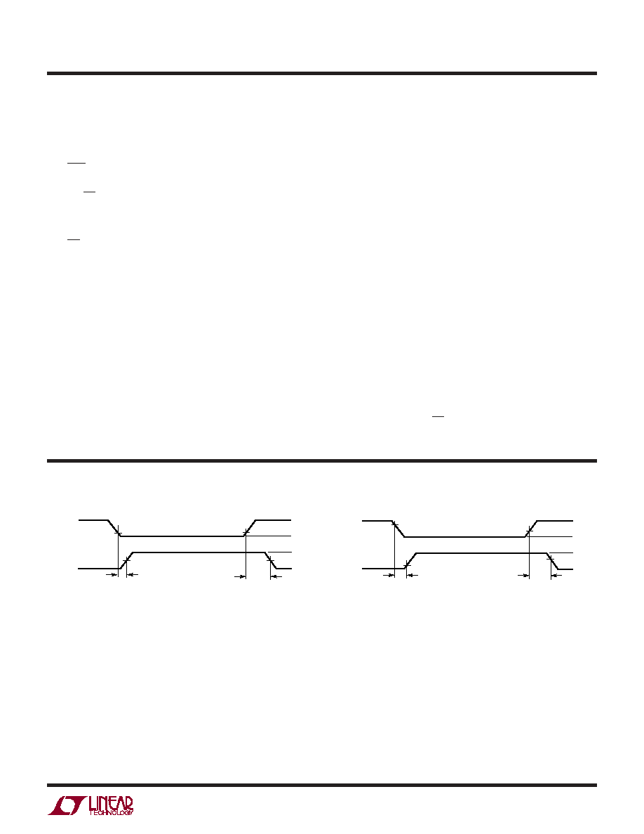
Figure 1. Driver Propagation Delay Timing
Figure 2. Receiver Propagation Delay Timing
1.4V
0V
VCC
0V
V+
V–
0V
DRIVER
INPUT
DRIVER
OUTPUT
1.4V
tHLD
tLHD
LTC1384 F01
0.8V
VCC
0V
2.4V
RX
INPUT
RX
OUTPUT
1.3V
tHLR
1.7V
tLHR
LTC1384 F02
VCC
0V
SWITCHI G TI E WAVEFOR S
UW
W
C1+, C1–, C2+, C2 –: Commutating Capacitor Inputs. These
pins require two external capacitors C = 0.1F: one from
C1+ to C1– and another from C2+ to C2 –. To maintain
charge pump efficiency, the capacitor’s effective series
resistance should be less than 2.
TR IN: RS232 Driver Input Pins. Inputs are TTL/CMOS
compatible. The inputs of unused drivers can be left
unconnected since 300k input pull-up resistors to VCC are
included on chip. To minimize power consumption, the
internal driver pull-up resistors are disconnected from VCC
in the Shutdown mode.
TR OUT: Driver Outputs at RS232 Voltage Levels. Outputs
are in a high impedance state when in the Shutdown or VCC
= 0V. The driver outputs are protected against ESD to
±10kV for human body model discharges.
RX IN: Receiver Inputs. These pins can be forced to ±25V
without damage. The receiver inputs are protected against
ESD to ±10kV for human body model discharges. Each
receiver provides 0.4V of hysteresis for noise immunity.
RX OUT: Receiver Outputs with TTL/CMOS Voltage Lev-
els. A logic high at RX EN puts the outputs into three-state.
UU
U
PI FU CTIO S
相关PDF资料 |
PDF描述 |
|---|---|
| IDT72231L10PF | IC FIFO SYNC 512X9 10NS 32QFP |
| MS3106A22-12P | CONN PLUG 5POS STRAIGHT W/PINS |
| LTC1382ISW#PBF | IC TXRX 5V RS232 W/SHTDWN 18SOIC |
| LTC1750IFW#TR | IC ADC 14BIT 80MSPS SMPL 48TSSOP |
| IDT72225LB15TFGI | IC FIFO 1024X18 SYNC 15NS 64TQFP |
相关代理商/技术参数 |
参数描述 |
|---|---|
| LTC1384IN#PBF | 功能描述:IC TXRX 5V RS232 LOW PWR 18-DIP RoHS:是 类别:集成电路 (IC) >> 接口 - 驱动器,接收器,收发器 系列:- 标准包装:27 系列:- 类型:收发器 驱动器/接收器数:3/3 规程:RS232,RS485 电源电压:4.75 V ~ 5.25 V 安装类型:表面贴装 封装/外壳:28-SOIC(0.295",7.50mm 宽) 供应商设备封装:28-SOIC 包装:管件 |
| LTC1384ISW | 功能描述:IC TXRX 5V RS232 LOW PWR 18-SOIC RoHS:否 类别:集成电路 (IC) >> 接口 - 驱动器,接收器,收发器 系列:- 标准包装:27 系列:- 类型:收发器 驱动器/接收器数:3/3 规程:RS232,RS485 电源电压:4.75 V ~ 5.25 V 安装类型:表面贴装 封装/外壳:28-SOIC(0.295",7.50mm 宽) 供应商设备封装:28-SOIC 包装:管件 |
| LTC1384ISW#PBF | 功能描述:IC TXRX 5V RS232 LOW PWR 18-SOIC RoHS:是 类别:集成电路 (IC) >> 接口 - 驱动器,接收器,收发器 系列:- 标准包装:27 系列:- 类型:收发器 驱动器/接收器数:3/3 规程:RS232,RS485 电源电压:4.75 V ~ 5.25 V 安装类型:表面贴装 封装/外壳:28-SOIC(0.295",7.50mm 宽) 供应商设备封装:28-SOIC 包装:管件 |
| LTC1384ISW#TR | 功能描述:IC TXRX RS232 5V LP SHTDN 18SOIC RoHS:否 类别:集成电路 (IC) >> 接口 - 驱动器,接收器,收发器 系列:- 标准包装:27 系列:- 类型:收发器 驱动器/接收器数:3/3 规程:RS232,RS485 电源电压:4.75 V ~ 5.25 V 安装类型:表面贴装 封装/外壳:28-SOIC(0.295",7.50mm 宽) 供应商设备封装:28-SOIC 包装:管件 |
| LTC1384ISW#TRPBF | 功能描述:IC TXRX 5V RS232 LOW PWR 18-SOIC RoHS:是 类别:集成电路 (IC) >> 接口 - 驱动器,接收器,收发器 系列:- 标准包装:27 系列:- 类型:收发器 驱动器/接收器数:3/3 规程:RS232,RS485 电源电压:4.75 V ~ 5.25 V 安装类型:表面贴装 封装/外壳:28-SOIC(0.295",7.50mm 宽) 供应商设备封装:28-SOIC 包装:管件 |
发布紧急采购,3分钟左右您将得到回复。