参数资料
| 型号: | LTC1390CN |
| 厂商: | Linear Technology |
| 文件页数: | 5/8页 |
| 文件大小: | 0K |
| 描述: | IC MULTIPLEXER 8X1 16DIP |
| 标准包装: | 25 |
| 功能: | 多路复用器 |
| 电路: | 1 x 8:1 |
| 导通状态电阻: | 255 欧姆 |
| 电压电源: | 单/双电源 |
| 电压 - 电源,单路/双路(±): | 3V,±5V |
| 电流 - 电源: | 200nA |
| 工作温度: | 0°C ~ 70°C |
| 安装类型: | 通孔 |
| 封装/外壳: | 16-DIP(0.300",7.62mm) |
| 供应商设备封装: | 16-PDIP |
| 包装: | 管件 |
5
LTC1390
sn1390 1390fs
PIN FUNCTIONS
UU
U
CS (Pin 11): Chip Select Input (TTL/CMOS Compatible). A
logic high on this input enables LTC1390 to read in the
channel selection bits and allow data transfer from Data 1
to Data 2. A logic low enables the desired channel for
analog signal transmission and allows data transfer from
Data 2 to Data 1.
Data 1 (Pin 12): Bidirectional Digital Input/Output (TTL/
CMOS Compatible). Input for the channel selection bits.
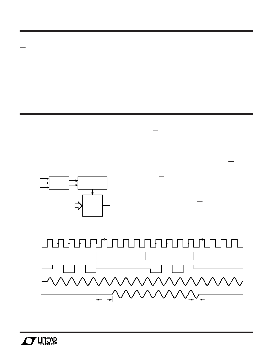
Figure 2: Multiplexer Operation
ANY
ANALOG
INPUTS
D
DATA 1
EN = HIGH
B2
B1
B0
EN = LOW
B2
B1
B0
LTC1390 F02
CLK
CS
tON
tOFF
APPLICATIO S I FOR ATIO
UU
W
U
When CS is high, the input data on the Data 1 pin is latched
into the 4-bit shift register on each rising clock edge. The
input data consists of an “EN” bit and a string of three bits
for channel selection. If “EN” bit is logic high as illustrated
in the first input data sequence, it enables the selected
channel. To ensure correct operation, the CS must be
pulled low before the next rising clock edge.
Once the CS is pulled low, all channels are simultaneously
switched off to ensure a break-before-make interval. After
a delay of tON, the selected channel is switched on allowing
signal transmission. The selected channel remains on
until the next falling edge of CS, and after a delay of tOFF,
it terminates the analog signal transmission and subse-
quently allows the selection of the next channel. If “EN” bit
is logic low, as illustrated in the second data sequence, it
disables all channels and there will be no analog signal
Multiplexer Operation
Figure 1 shows the block diagram of the components
within the LTC1390 required for MUX operation. The
LTC1390 uses Data 1 to select its 8 channels and a chip
select input CS to switch on the selected channel as shown
in Figure 2.
4-BIT SHIFT
REGISTER
CLK
DATA 1
CS
CONTROL
LOGIC
MUX
BLOCK
ANALOG
INPUT
ANALOG
OUTPUT
LTC1390 F01
Figure 1: Simplified Block Diagram of the MUX Operation
Data 2 (Pin 13): Bidirectional Digital Input/Output (TTL/
CMOS Compatible).
V – (Pin 14): Negative Supply. For
±5V dual supply appli-
cations, |V–| should not exceed |V+| by more than 20% for
proper channel selection.
D (Pin 15): Analog Multiplexer Output/Analog
Demultiplexer Input.
V+ (Pin 16): Positive Supply.
相关PDF资料 |
PDF描述 |
|---|---|
| LTC1391IGN#TRPBF | IC MULTIPLEXER 8X1 16SSOP |
| LTC1393IGN#PBF | IC MULTIPLEXER DUAL 4X1 16SSOP |
| LTC1480IS8#TRPBF | IC TXRX 3.3V RS485 LOWPWR 8-SOIC |
| LTC1481IS8#TRPBF | IC TXRX RS485 LOPWR W/SHTDN8SOIC |
| LTC1483IS8#TRPBF | IC TXRX RS485 LOW EMI LOPWR8SOIC |
相关代理商/技术参数 |
参数描述 |
|---|---|
| LTC1390CN#PBF | 功能描述:IC MULTIPLEXER 8X1 16DIP RoHS:是 类别:集成电路 (IC) >> 接口 - 模拟开关,多路复用器,多路分解器 系列:- 标准包装:1,000 系列:- 功能:多路复用器 电路:1 x 4:1 导通状态电阻:- 电压电源:双电源 电压 - 电源,单路/双路(±):±5V 电流 - 电源:7mA 工作温度:-40°C ~ 85°C 安装类型:表面贴装 封装/外壳:16-SOIC(0.154",3.90mm 宽) 供应商设备封装:16-SOIC 包装:带卷 (TR) |
| LTC1390CS | 制造商:Linear Technology 功能描述:Analog Multiplexer Single 8:1 16-Pin SOIC N |
| LTC1390CS#PBF | 功能描述:IC MULTIPLEXER 8X1 16SOIC RoHS:是 类别:集成电路 (IC) >> 接口 - 模拟开关,多路复用器,多路分解器 系列:- 特色产品:MicroPak? 标准包装:1 系列:- 功能:开关 电路:2 x SPST - NC 导通状态电阻:500 毫欧 电压电源:单电源 电压 - 电源,单路/双路(±):1.4 V ~ 4.3 V 电流 - 电源:150nA 工作温度:-40°C ~ 125°C 安装类型:表面贴装 封装/外壳:8-XFDFN 供应商设备封装:8-XSON,SOT833-1 (1.95x1) 包装:Digi-Reel® 其它名称:568-5557-6 |
| LTC1390CS#TR | 功能描述:IC MULTIPLEXER 8X1 16SOIC RoHS:否 类别:集成电路 (IC) >> 接口 - 模拟开关,多路复用器,多路分解器 系列:- 标准包装:1,000 系列:- 功能:多路复用器 电路:1 x 4:1 导通状态电阻:- 电压电源:双电源 电压 - 电源,单路/双路(±):±5V 电流 - 电源:7mA 工作温度:-40°C ~ 85°C 安装类型:表面贴装 封装/外壳:16-SOIC(0.154",3.90mm 宽) 供应商设备封装:16-SOIC 包装:带卷 (TR) |
| LTC1390CS#TRPBF | 功能描述:IC MULTIPLEXER 8X1 16SOIC RoHS:是 类别:集成电路 (IC) >> 接口 - 模拟开关,多路复用器,多路分解器 系列:- 标准包装:1,000 系列:- 功能:多路复用器 电路:1 x 4:1 导通状态电阻:- 电压电源:双电源 电压 - 电源,单路/双路(±):±5V 电流 - 电源:7mA 工作温度:-40°C ~ 85°C 安装类型:表面贴装 封装/外壳:16-SOIC(0.154",3.90mm 宽) 供应商设备封装:16-SOIC 包装:带卷 (TR) |
发布紧急采购,3分钟左右您将得到回复。