- 您现在的位置:买卖IC网 > PDF目录179916 > LTC1391CS#TRPBF (LINEAR TECHNOLOGY CORP) 8-Channel Analog Multiplexer with Cascadable Serial Interface; Package: SO; No of Pins: 16; Temperature Range: 0°C to +70°C PDF资料下载
参数资料
| 型号: | LTC1391CS#TRPBF |
| 厂商: | LINEAR TECHNOLOGY CORP |
| 元件分类: | 多路复用及模拟开关 |
| 英文描述: | 8-Channel Analog Multiplexer with Cascadable Serial Interface; Package: SO; No of Pins: 16; Temperature Range: 0°C to +70°C |
| 中文描述: | 8-CHANNEL, SGL ENDED MULTIPLEXER, PDSO16 |
| 封装: | 0.150 INCH, PLASTIC, SOP-16 |
| 文件页数: | 9/12页 |
| 文件大小: | 175K |
| 代理商: | LTC1391CS#TRPBF |
6
LTC1391
sn1391 1391fas
APPLICATIONS INFORMATION
WU
U
Multiplexer Operation
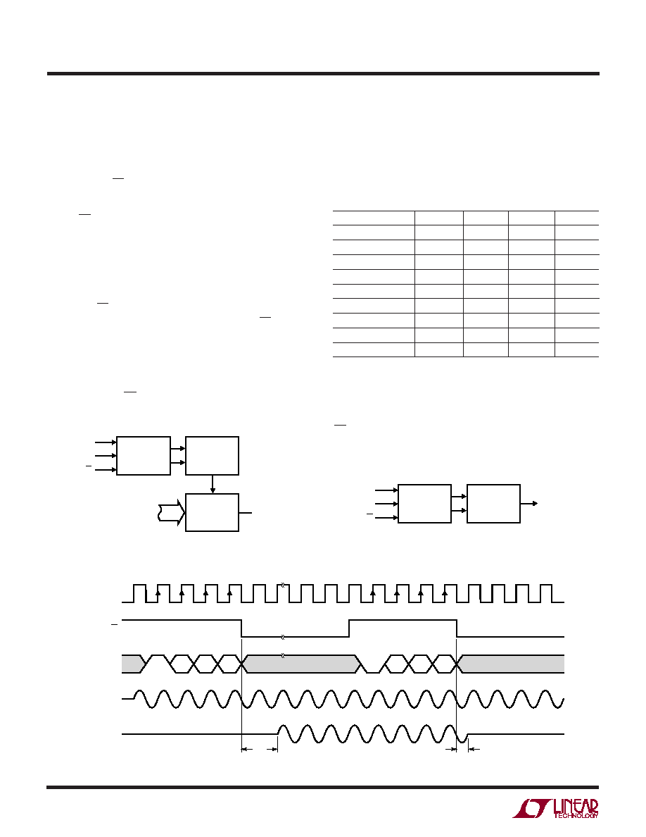
Figure 1 shows the block diagram of the components
within the LTC1391 required for MUX operation. The
LTC1391 uses DIN to select the active channel and the chip
select input, CS, to switch on the selected channel as
shown in Figure 2.
When CS is high, the input data on the DIN pin is latched
into the 4-bit shift register on the rising clock edge. The
input data consists of the “EN” bit and a string of three bits
for channel selection. If “EN” bit is logic high as illustrated
in the first input data sequence, it enables the selected
channel. After the clocking in of the last channel selection
bit B0, the CS pin must be pulled low before the next rising
clock edge to ensure correct operation. Once CS is pulled
low, the previously selected channel is switched off to
ensure a break-before-make interval. After a delay of tON,
the selected channel is switched on allowing signal trans-
mission. The selected channel remains on until the next
falling edge of CS. After a delay of tOFF, the LTC1391
terminates the analog signal transmission and allows the
selection of next channel. If the “EN” bit is logic low, as
illustrated in the second data sequence, it disables all
channels and there will be no analog signal transmission.
Table 1 shows the various bit combinations for channel
selection.
Table 1. Logic Table for Channel Selection
ACTIVE CHANNEL
EN
B2
B1
BO
All Off
0
X
S0
1
0
S1
1
0
1
S2
1
0
1
0
S3
1
0
1
S4
1
0
S5
1
0
1
S6
1
0
S7
1
Digital Data Transfer Operation
The block diagram of Figure 3 shows the components
within the LTC1391 required for serial data transfer. When
CS is held high, data is fed into the 4-bit shift register and
then shifted to DOUT. Data appears at DOUT after the fourth
rising edge of the clock as shown in Figure 4. The last four
Figure 2. Multiplexer Operation
EN
HIGH
B2
EN LO
B2
B1
B0
B1
B0
CLK
CS
DIN
ANY ANALOG
INPUT
D
tON
tOFF
1391 F02
Figure 1. Simplified Block Diagram of the MUX Operation
CONTROL
LOGIC
4-BIT SHIFT
REGISTER
MUX
BLOCK
CLK
DIN
CS
1391 F01
ANALOG
OUTPUT (D)
ANALOG INPUTS
(S0 TO S7)
Figure 3. Simplified Block Diagram of the
Digital Data Transfer Operation
CONTROL
LOGIC
4-BIT SHIFT
REGISTER
CLK
DIN
CS
1391 F03
DOUT
相关PDF资料 |
PDF描述 |
|---|---|
| LTC1391IGN#PBF | 8-Channel Analog Multiplexer with Cascadable Serial Interface; Package: SSOP; No of Pins: 16; Temperature Range: -40°C to +85°C |
| LTC1391CS#PBF | 8-Channel Analog Multiplexer with Cascadable Serial Interface; Package: SO; No of Pins: 16; Temperature Range: 0°C to +70°C |
| LTC1391IGN#TRPBF | 8-Channel Analog Multiplexer with Cascadable Serial Interface; Package: SSOP; No of Pins: 16; Temperature Range: -40°C to +85°C |
| LTC1391IS#PBF | 8-Channel Analog Multiplexer with Cascadable Serial Interface; Package: SO; No of Pins: 16; Temperature Range: -40°C to +85°C |
| LTC1391IS#TRPBF | 8-Channel Analog Multiplexer with Cascadable Serial Interface; Package: SO; No of Pins: 16; Temperature Range: -40°C to +85°C |
相关代理商/技术参数 |
参数描述 |
|---|---|
| LTC1391IGN | 功能描述:IC MULTIPLEXER 8X1 16SSOP RoHS:否 类别:集成电路 (IC) >> 接口 - 模拟开关,多路复用器,多路分解器 系列:- 其它有关文件:STG4159 View All Specifications 标准包装:5,000 系列:- 功能:开关 电路:1 x SPDT 导通状态电阻:300 毫欧 电压电源:双电源 电压 - 电源,单路/双路(±):±1.65 V ~ 4.8 V 电流 - 电源:50nA 工作温度:-40°C ~ 85°C 安装类型:表面贴装 封装/外壳:7-WFBGA,FCBGA 供应商设备封装:7-覆晶 包装:带卷 (TR) |
| LTC1391IGN#PBF | 功能描述:IC MULTIPLEXER 8X1 16SSOP RoHS:是 类别:集成电路 (IC) >> 接口 - 模拟开关,多路复用器,多路分解器 系列:- 其它有关文件:STG4159 View All Specifications 标准包装:5,000 系列:- 功能:开关 电路:1 x SPDT 导通状态电阻:300 毫欧 电压电源:双电源 电压 - 电源,单路/双路(±):±1.65 V ~ 4.8 V 电流 - 电源:50nA 工作温度:-40°C ~ 85°C 安装类型:表面贴装 封装/外壳:7-WFBGA,FCBGA 供应商设备封装:7-覆晶 包装:带卷 (TR) |
| LTC1391IGN#TR | 功能描述:IC MULTIPLEXER 8X1 16SSOP RoHS:否 类别:集成电路 (IC) >> 接口 - 模拟开关,多路复用器,多路分解器 系列:- 其它有关文件:STG4159 View All Specifications 标准包装:5,000 系列:- 功能:开关 电路:1 x SPDT 导通状态电阻:300 毫欧 电压电源:双电源 电压 - 电源,单路/双路(±):±1.65 V ~ 4.8 V 电流 - 电源:50nA 工作温度:-40°C ~ 85°C 安装类型:表面贴装 封装/外壳:7-WFBGA,FCBGA 供应商设备封装:7-覆晶 包装:带卷 (TR) |
| LTC1391IGN#TRPBF | 功能描述:IC MULTIPLEXER 8X1 16SSOP RoHS:是 类别:集成电路 (IC) >> 接口 - 模拟开关,多路复用器,多路分解器 系列:- 其它有关文件:STG4159 View All Specifications 标准包装:5,000 系列:- 功能:开关 电路:1 x SPDT 导通状态电阻:300 毫欧 电压电源:双电源 电压 - 电源,单路/双路(±):±1.65 V ~ 4.8 V 电流 - 电源:50nA 工作温度:-40°C ~ 85°C 安装类型:表面贴装 封装/外壳:7-WFBGA,FCBGA 供应商设备封装:7-覆晶 包装:带卷 (TR) |
| LTC1391IS | 功能描述:IC MULTIPLEXER 8X1 16SOIC RoHS:否 类别:集成电路 (IC) >> 接口 - 模拟开关,多路复用器,多路分解器 系列:- 标准包装:1,000 系列:- 功能:多路复用器 电路:1 x 4:1 导通状态电阻:- 电压电源:双电源 电压 - 电源,单路/双路(±):±5V 电流 - 电源:7mA 工作温度:-40°C ~ 85°C 安装类型:表面贴装 封装/外壳:16-SOIC(0.154",3.90mm 宽) 供应商设备封装:16-SOIC 包装:带卷 (TR) |
发布紧急采购,3分钟左右您将得到回复。