- 您现在的位置:买卖IC网 > PDF目录2003 > LTC1402IGN#TRPBF (Linear Technology)IC ADC 12BIT 2.2MSPS SHDN 16SSOP PDF资料下载
参数资料
| 型号: | LTC1402IGN#TRPBF |
| 厂商: | Linear Technology |
| 文件页数: | 9/24页 |
| 文件大小: | 0K |
| 描述: | IC ADC 12BIT 2.2MSPS SHDN 16SSOP |
| 标准包装: | 2,500 |
| 位数: | 12 |
| 采样率(每秒): | 2.2M |
| 数据接口: | MICROWIRE?,串行,SPI? |
| 转换器数目: | 1 |
| 功率耗散(最大): | 150mW |
| 电压电源: | 模拟和数字,双 ± |
| 工作温度: | -40°C ~ 85°C |
| 安装类型: | 表面贴装 |
| 封装/外壳: | 16-SSOP(0.154",3.90mm 宽) |
| 供应商设备封装: | 16-SSOP |
| 包装: | 带卷 (TR) |
| 输入数目和类型: | 2 个单端,单极;2 个单端,双极;1 个差分,单极;1 个差分,双极 |
17
LTC1402
APPLICATIONS INFORMATION
WU
U
edge of CONV. Please note the delay specification from
SCK to a valid DOUT. DOUT is always guaranteed to be valid
by the next rising edge of SCK.
DIGITAL JITTER AT CONV (PIN 16)
In high speed applications, where high amplitude sinewaves
above 100kHz are sampled, the CONV signal must have as
little jitter as possible (10ps or less). The square wave
output of a common crystal clock module usually meets
this requirement easily. The challenge is to generate a CONV
signal from this crystal clock without jitter corruption from
other digital circuits in the system. A clock divider and any
gates in the signal path from the crystal clock to the CONV
input should not share the same integrated circuit with
other parts of the system. As shown in the interface circuit
examples, the LTC1402’s SCK and CONV inputs should be
driven first with digital buffers used to drive the serial port
interface. Also note that the master clock in the DSP may
already be corrupted with jitter, even if it comes directly
from the DSP crystal. Another problem with high speed
processor clocks is that they often use a low cost, low
speed crystal (i.e., 10MHz) to generated a fast, but jittery,
phase locked loop system clock (i.e., 40MHz). The jitter, in
these PLL-generated high speed clocks, can be several
nanoseconds. Note that if you choose to use the frame
sync signal generated by the DSP port, this signal will have
the same jitter of the DSP’s master clock.
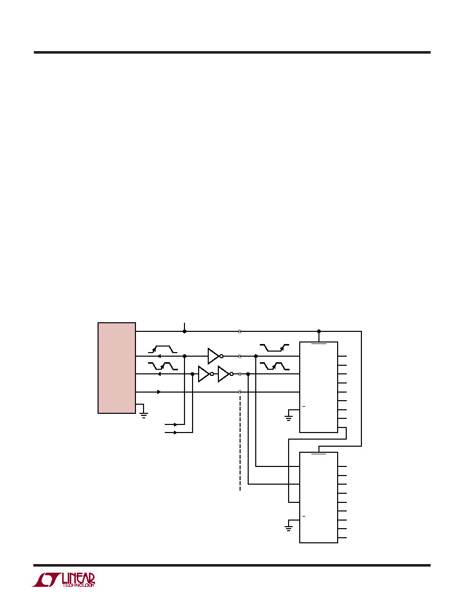
SERIAL TO PARALLEL CONVERSION
You can take advantage of the serial interface of the LTC1402
in a parallel data system to minimize bus wiring conges-
tion in the PC board layout. Figure 13 shows an example
of this interface. It is best to send the SCK and CONV
signals to the LTC1402, and then bus them together across
the board to avoid excessive time skew among the three
signals. It is usually not necessary to buffer DOUT, if the PC
track is not too long. Buffering SCK and CONV prevents
jitter from corrupting these signals. The relative phase
between SCK and CONV affects the position of the parallel
word at the output of the 74HC595. The position of the
output word in Figure 13 assumes 16 clocks between each
CONV rising edge, and the CONV pulse is one clock wide.
Figure 13. Serial to Parallel Interface
SRCLR
QA
QB
QC
QD
QE
QF
QG
RCK
SRCK
SER
G
QH
′
15
1
2
3
4
5
6
12
10
11
14
13
7
9
SRCLR
QA
QB
QC
QD
QE
QF
QG
RCK
74ACT04
SRCK
SER
74HC595
G
11
5V
16
15
10
9
3-WIRE SERIAL
INTERFACE LINK
QH
′
15
1
2
3
4
5
6
12
11
14
13
1402 F13
7
D0
D1
D2
D3
D4
D5
D7
D8
D9
D10
D11
REFRDY
D6
9
OVDD
CONV
SCK
LTC1402
DOUT
OGND
CONV
CLK
相关PDF资料 |
PDF描述 |
|---|---|
| LTC1403AHMSE#TRPBF | IC ADC 14BIT 2.8MSPS DIFF 10MSOP |
| LTC1403AIMSE-1#TRPBF | IC ADC 14BIT 2.8MSPS DIFF 10MSOP |
| LTC1404IS8#TRPBF | IC A/D CONV 12BIT W/SHTDN 8-SOIC |
| LTC1405IGN#TRPBF | IC ADC 12BIT 5MSPS SAMPLE 28SSOP |
| LTC1406IGN#TRPBF | IC A/D CONV 8BIT SAMPLING 24SSOP |
相关代理商/技术参数 |
参数描述 |
|---|---|
| LTC1403ACMSE | 功能描述:IC ADC 14BIT 2.8MSPS DIFF 10MSOP RoHS:否 类别:集成电路 (IC) >> 数据采集 - 模数转换器 系列:- 标准包装:1,000 系列:- 位数:16 采样率(每秒):45k 数据接口:串行 转换器数目:2 功率耗散(最大):315mW 电压电源:模拟和数字 工作温度:0°C ~ 70°C 安装类型:表面贴装 封装/外壳:28-SOIC(0.295",7.50mm 宽) 供应商设备封装:28-SOIC W 包装:带卷 (TR) 输入数目和类型:2 个单端,单极 |
| LTC1403ACMSE#PBF | 功能描述:IC ADC 14BIT 2.8MSPS 10-MSOP RoHS:是 类别:集成电路 (IC) >> 数据采集 - 模数转换器 系列:- 标准包装:1 系列:microPOWER™ 位数:8 采样率(每秒):1M 数据接口:串行,SPI? 转换器数目:1 功率耗散(最大):- 电压电源:模拟和数字 工作温度:-40°C ~ 125°C 安装类型:表面贴装 封装/外壳:24-VFQFN 裸露焊盘 供应商设备封装:24-VQFN 裸露焊盘(4x4) 包装:Digi-Reel® 输入数目和类型:8 个单端,单极 产品目录页面:892 (CN2011-ZH PDF) 其它名称:296-25851-6 |
| LTC1403ACMSE#PBF | 制造商:Linear Technology 功能描述:ADC, 14BIT, 2.8MSPS, MSOP-10 |
| LTC1403ACMSE#TR | 功能描述:IC ADC 14BIT 2.8MSPS DIFF 10MSOP RoHS:否 类别:集成电路 (IC) >> 数据采集 - 模数转换器 系列:- 标准包装:1,000 系列:- 位数:16 采样率(每秒):45k 数据接口:串行 转换器数目:2 功率耗散(最大):315mW 电压电源:模拟和数字 工作温度:0°C ~ 70°C 安装类型:表面贴装 封装/外壳:28-SOIC(0.295",7.50mm 宽) 供应商设备封装:28-SOIC W 包装:带卷 (TR) 输入数目和类型:2 个单端,单极 |
| LTC1403ACMSE#TRPBF | 功能描述:IC ADC 14BIT 2.8MSPS DIFF 10MSOP RoHS:是 类别:集成电路 (IC) >> 数据采集 - 模数转换器 系列:- 标准包装:1,000 系列:- 位数:16 采样率(每秒):45k 数据接口:串行 转换器数目:2 功率耗散(最大):315mW 电压电源:模拟和数字 工作温度:0°C ~ 70°C 安装类型:表面贴装 封装/外壳:28-SOIC(0.295",7.50mm 宽) 供应商设备封装:28-SOIC W 包装:带卷 (TR) 输入数目和类型:2 个单端,单极 |
发布紧急采购,3分钟左右您将得到回复。