- 您现在的位置:买卖IC网 > PDF目录10257 > LTC1402IGN (Linear Technology)IC ADC 12BIT 2.2MSPS SHDN 16SSOP PDF资料下载
参数资料
| 型号: | LTC1402IGN |
| 厂商: | Linear Technology |
| 文件页数: | 5/24页 |
| 文件大小: | 0K |
| 描述: | IC ADC 12BIT 2.2MSPS SHDN 16SSOP |
| 标准包装: | 100 |
| 位数: | 12 |
| 采样率(每秒): | 2.2M |
| 数据接口: | MICROWIRE?,串行,SPI? |
| 转换器数目: | 1 |
| 功率耗散(最大): | 150mW |
| 电压电源: | 模拟和数字,双 ± |
| 工作温度: | -40°C ~ 85°C |
| 安装类型: | 表面贴装 |
| 封装/外壳: | 16-SSOP(0.154",3.90mm 宽) |
| 供应商设备封装: | 16-SSOP |
| 包装: | 管件 |
| 输入数目和类型: | 2 个单端,单极;2 个单端,双极;1 个差分,单极;1 个差分,双极 |
13
LTC1402
APPLICATIONS INFORMATION
WU
U
all the internal references. When AGND2 (Pin 6) is tied to
the external ground plane, it sources 2.7mA
±30% typi-
cally; approximately 2mA are sourced through an internal
equivalent 2k resistance tied to the VREF (Pin 5) at 4.096V
and the remaining 0.7mA supply the internal reference
ground. The VREF (Pin 5) equivalent input resistance is the
same 2k tied to AGND2 (Pin 6). When you bus a common
reference voltage to several LTC1402 ADCs, you need to
keep PC board track resistance low to avoid reference
voltage attenuation at each ADC. For example, 0.5
of
track resistance to Pins 5 or 6 causes 0.025% of reference
voltage and input range reduction. Figure 8 shows op-
tional buffer amplifiers at each ADC to eliminate resistive
voltage drops from the common external reference to each
ADC. Figure 8 shows 10
F bypass capacitors tied to the
common analog ground plane, at VREF (Pin 5) and AGND2
(Pin 6), wired closely to each ADC to eliminate crosstalk of
internal ADC glitch currents from one ADC to another. The
10
F bypass capacitors are recommended whether you
drive Pins 5 and 6 with amplifiers, or with copper traces
INPUT SPAN VERSUS REFERENCE VOLTAGE
The differential input range has a voltage span that equals
the difference between the voltage at the reference buffer
output VREF at Pin 5, and the voltage at the reference
ground AGND2 at Pin 6. The external reference voltage
may have any value between 2V and 5V. The internal ADC
is referenced to these two points. If you use an external
reference, tie the GAIN (Pin 7) to AVDD (Pin 1) to disable
the internal reference, and connect the external reference
between VREF (Pin 5) and AGND2 (Pin 6).
If you cut the reference voltage in half by halving the gain
of the reference buffer with the GAIN (Pin 7) tied to VREF
(Pin 5), the input span also cuts in half. In bipolar mode,
the differential input range changes from
±2.048V to
±1.024V, when the reference is cut in half. In unipolar
mode, the differential input range changes from 0V-
4.096V to 0V-2.048V, for the same reference cut in half.
Note that in both unipolar and bipolar modes, the input
range pivots around 0V with changing reference voltage.
AGND2 (Pin 6) has no direct effect on the ADC offset
voltage, it only affects input voltage span. Any external
offsetting voltages must be applied through the AIN+ and
AIN– inputs, as shown in Figure 10b.
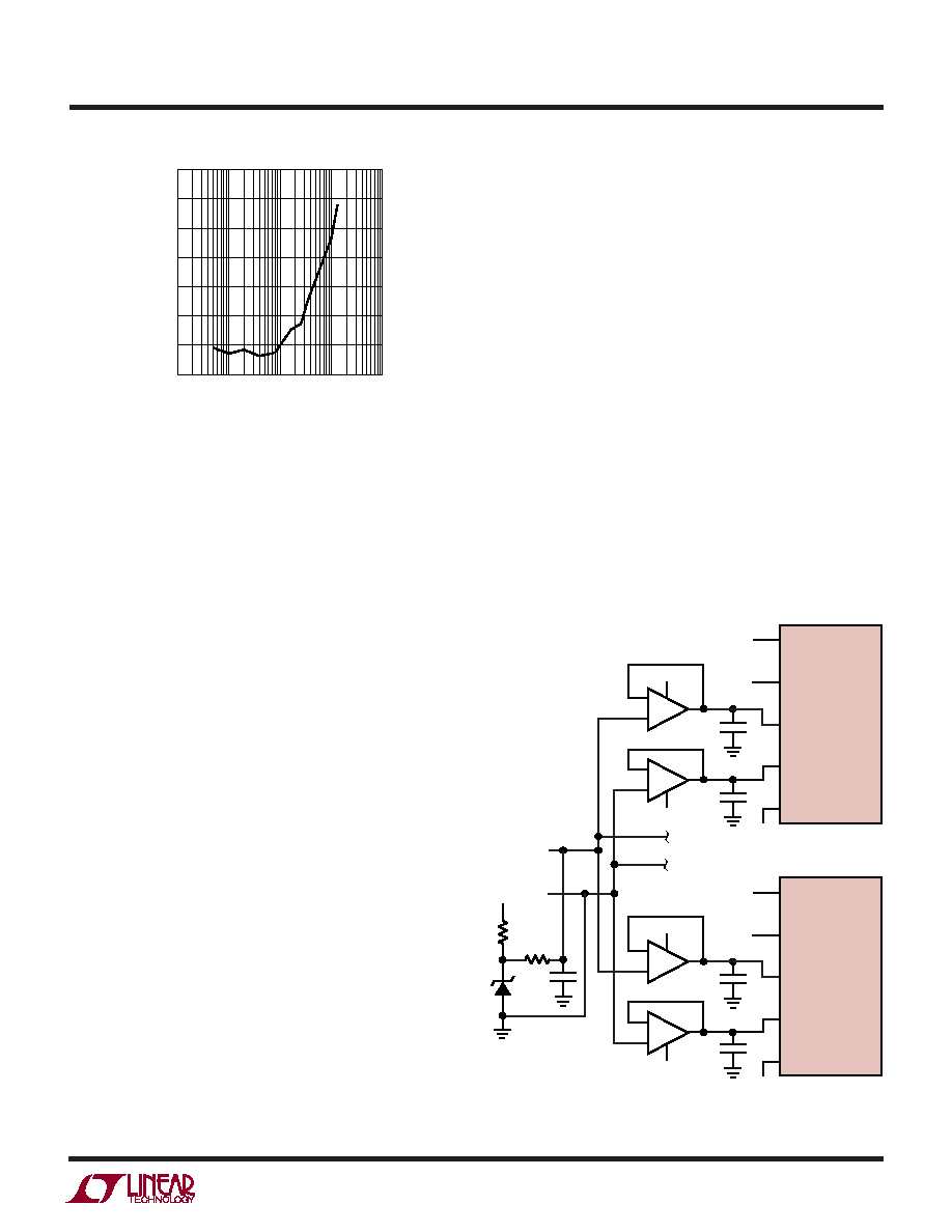
SEVERAL LTC1402 ADCs MAY SHARE ONE
EXTERNAL REFERENCE
Figure 8 shows how several ADCs can share a single
common external reference. The VREF (Pin 5) and AGND2
(Pin 6) of several LTC1402 ADCs can be tied together to
share the same external reference in a data acquisition
system. Tie GAIN (Pin 7) to AVDD at each ADC to disable
Figure 8. Several LTC1402 ADCs Can Share a Single
External Reference
FREQUENCY (MHz)
–40
AMPLITUDE
(dB) –30
–20
–10
0
0.1
10
100
1000
1402 F07
–50
–60
–70
1
Figure 7. CMRR vs Input Frequency
LTC1402
AIN
+
5V
AIN
–
VREF
AGND2
GAIN
1402 F08
3
2
5
6
7
10
F
10
F
+
–
+
–
2
6
3
5
5V
–5V
4
1
8
7
LTC1402
AIN
+
ANALOG
INPUTS
ANALOG
INPUTS
5V
AIN
–
VREF
AGND2
GAIN
3
2
5
6
7
10
F
10
F
+
–
+
–
2
6
3
5
5V
–5V
4
1
8
7
4.096V
1/2 LT1368CS8
0.1
F
10k
1k
5V
LT1634AI-4.096
相关PDF资料 |
PDF描述 |
|---|---|
| VI-26N-MY | CONVERTER MOD DC/DC 18.5V 50W |
| VI-22J-IW-S | CONVERTER MOD DC/DC 36V 100W |
| 14380-10SG-300 | CONN RCPT 10POS PNL MNT SKT |
| AD7705BN | IC ADC 16BIT 2CH 16-DIP |
| VI-2NB-IU-S | CONVERTER MOD DC/DC 95V 200W |
相关代理商/技术参数 |
参数描述 |
|---|---|
| LTC1402IGN#PBF | 功能描述:IC ADC 12BIT 2.2MSPS SHDN 16SSOP RoHS:是 类别:集成电路 (IC) >> 数据采集 - 模数转换器 系列:- 标准包装:1,000 系列:- 位数:16 采样率(每秒):45k 数据接口:串行 转换器数目:2 功率耗散(最大):315mW 电压电源:模拟和数字 工作温度:0°C ~ 70°C 安装类型:表面贴装 封装/外壳:28-SOIC(0.295",7.50mm 宽) 供应商设备封装:28-SOIC W 包装:带卷 (TR) 输入数目和类型:2 个单端,单极 |
| LTC1402IGN#TR | 功能描述:IC ADC 12BIT 2.2MSPS SHDN 16SSOP RoHS:否 类别:集成电路 (IC) >> 数据采集 - 模数转换器 系列:- 标准包装:1,000 系列:- 位数:16 采样率(每秒):45k 数据接口:串行 转换器数目:2 功率耗散(最大):315mW 电压电源:模拟和数字 工作温度:0°C ~ 70°C 安装类型:表面贴装 封装/外壳:28-SOIC(0.295",7.50mm 宽) 供应商设备封装:28-SOIC W 包装:带卷 (TR) 输入数目和类型:2 个单端,单极 |
| LTC1402IGN#TRPBF | 功能描述:IC ADC 12BIT 2.2MSPS SHDN 16SSOP RoHS:是 类别:集成电路 (IC) >> 数据采集 - 模数转换器 系列:- 标准包装:1,000 系列:- 位数:16 采样率(每秒):45k 数据接口:串行 转换器数目:2 功率耗散(最大):315mW 电压电源:模拟和数字 工作温度:0°C ~ 70°C 安装类型:表面贴装 封装/外壳:28-SOIC(0.295",7.50mm 宽) 供应商设备封装:28-SOIC W 包装:带卷 (TR) 输入数目和类型:2 个单端,单极 |
| LTC1403ACMSE | 功能描述:IC ADC 14BIT 2.8MSPS DIFF 10MSOP RoHS:否 类别:集成电路 (IC) >> 数据采集 - 模数转换器 系列:- 标准包装:1,000 系列:- 位数:16 采样率(每秒):45k 数据接口:串行 转换器数目:2 功率耗散(最大):315mW 电压电源:模拟和数字 工作温度:0°C ~ 70°C 安装类型:表面贴装 封装/外壳:28-SOIC(0.295",7.50mm 宽) 供应商设备封装:28-SOIC W 包装:带卷 (TR) 输入数目和类型:2 个单端,单极 |
| LTC1403ACMSE#PBF | 功能描述:IC ADC 14BIT 2.8MSPS 10-MSOP RoHS:是 类别:集成电路 (IC) >> 数据采集 - 模数转换器 系列:- 标准包装:1 系列:microPOWER™ 位数:8 采样率(每秒):1M 数据接口:串行,SPI? 转换器数目:1 功率耗散(最大):- 电压电源:模拟和数字 工作温度:-40°C ~ 125°C 安装类型:表面贴装 封装/外壳:24-VFQFN 裸露焊盘 供应商设备封装:24-VQFN 裸露焊盘(4x4) 包装:Digi-Reel® 输入数目和类型:8 个单端,单极 产品目录页面:892 (CN2011-ZH PDF) 其它名称:296-25851-6 |
发布紧急采购,3分钟左右您将得到回复。