- 您现在的位置:买卖IC网 > PDF目录10226 > LTC1410ISW#TRPBF (Linear Technology)IC A/D CONV 12BIT SAMPLNG 28SOIC PDF资料下载
参数资料
| 型号: | LTC1410ISW#TRPBF |
| 厂商: | Linear Technology |
| 文件页数: | 14/16页 |
| 文件大小: | 0K |
| 描述: | IC A/D CONV 12BIT SAMPLNG 28SOIC |
| 标准包装: | 1,000 |
| 位数: | 12 |
| 采样率(每秒): | 1.25M |
| 数据接口: | 并联 |
| 转换器数目: | 1 |
| 功率耗散(最大): | 230mW |
| 电压电源: | 双 ± |
| 工作温度: | -40°C ~ 85°C |
| 安装类型: | 表面贴装 |
| 封装/外壳: | 28-SOIC(0.295",7.50mm 宽) |
| 供应商设备封装: | 28-SOIC |
| 包装: | 带卷 (TR) |
| 输入数目和类型: | 2 个单端,双极;1 个差分,双极 |
7
LTC1410
TEST CIRCUITS
APPLICATIONS INFORMATION
WU
U
CONVERSION DETAILS
The LTC1410 uses a successive approximation algorithm
and an internal sample-and-hold circuit to convert an
analog signal to a 12-bit parallel output. The ADC is
complete with a precision reference and an internal clock.
The control logic provides easy interface to microproces-
sors and DSPs. (Please refer to the Digital Interface
section for the data format.)
Conversion start is controlled by the CS and CONVST
inputs. At the start of the conversion the successive
approximation register (SAR) is reset. Once a conversion
cycle has begun it cannot be restarted.
During the conversion, the internal differential 12-bit
capacitive DAC output is sequenced by the SAR from the
Most Significant Bit (MSB) to the Least Significant Bit
(LSB). Referring to Figure 1, the + AIN and – AIN inputs are
connected to the sample-and-hold capacitors (CSAMPLE)
during the acquire phase and the comparator offset is
nulled by the zeroing switches. In this acquire phase, a
minimum duration of 100ns will provide enough time for
the sample-and-hold capacitors to acquire the analog
signal. During the convert phase the comparator zeroing
switches open, putting the comparator into compare
mode. The input switches connect the CSAMPLE capacitors
to ground, transferring the differential analog input charge
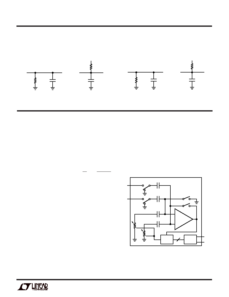
1k
CL
DBN
(A) Hi-Z TO VOH AND VOL TO VOH
(B) Hi-Z TO VOL AND VOH TO VOL
DBN
1k
5V
1410 TC01
1k
100pF
DBN
(A) VOH TO Hi-Z
(B) VOL TO Hi-Z
DBN
1k
5V
1410 TC02
Load Circuits for Access Timing
Load Circuits for Output Float Delay
onto the summing junctions. This input charge is succes-
sively compared with the binarily-weighted charges sup-
plied by the differential capacitive DAC. Bit decisions are
made by the high speed comparator. At the end of a
conversion, the differential DAC output balances the + AIN
and – AIN input charges. The SAR contents (a 12-bit data
word) which represent the difference of + AIN and – AIN are
loaded into the 12-bit output latches.
SAMPLE
HOLD
+CSAMPLE
–CSAMPLE
D11
D0
ZEROING SWITCHES
+AIN
+CDAC
+VDAC
–CDAC
–VDAC
–AIN
12
1410 F01
COMP
+
–
OUTPUT
LATCHES
SAR
SAMPLE
HOLD
Figure 1. Simplified Block Diagram
相关PDF资料 |
PDF描述 |
|---|---|
| LTC1415ISW#PBF | IC A/D CONV 12BIT SAMPLNG 28SOIC |
| SP3224ECA-L/TR | IC TXRX RS232 ESD SD 20SSOP |
| LTC1415ISW | IC ADC 12BIT 1.25MSPS 28-SOIC |
| MS27467T13F4P | CONN PLUG 4POS STRAIGHT W/PINS |
| VI-21N-IU-F3 | CONVERTER MOD DC/DC 18.5V 200W |
相关代理商/技术参数 |
参数描述 |
|---|---|
| LTC1411CG | 功能描述:IC A/D CONV 14BIT 2.5MSPS 36SSOP RoHS:否 类别:集成电路 (IC) >> 数据采集 - 模数转换器 系列:- 标准包装:1 系列:- 位数:14 采样率(每秒):83k 数据接口:串行,并联 转换器数目:1 功率耗散(最大):95mW 电压电源:双 ± 工作温度:0°C ~ 70°C 安装类型:通孔 封装/外壳:28-DIP(0.600",15.24mm) 供应商设备封装:28-PDIP 包装:管件 输入数目和类型:1 个单端,双极 |
| LTC1411CG#PBF | 功能描述:IC ADC 14BIT 2.5MSPS 36SSOP RoHS:是 类别:集成电路 (IC) >> 数据采集 - 模数转换器 系列:- 标准包装:1 系列:- 位数:14 采样率(每秒):83k 数据接口:串行,并联 转换器数目:1 功率耗散(最大):95mW 电压电源:双 ± 工作温度:0°C ~ 70°C 安装类型:通孔 封装/外壳:28-DIP(0.600",15.24mm) 供应商设备封装:28-PDIP 包装:管件 输入数目和类型:1 个单端,双极 |
| LTC1411CG#TR | 功能描述:IC A/D CONV 14BIT 2.5MSPS 36SSOP RoHS:否 类别:集成电路 (IC) >> 数据采集 - 模数转换器 系列:- 标准包装:1 系列:- 位数:14 采样率(每秒):83k 数据接口:串行,并联 转换器数目:1 功率耗散(最大):95mW 电压电源:双 ± 工作温度:0°C ~ 70°C 安装类型:通孔 封装/外壳:28-DIP(0.600",15.24mm) 供应商设备封装:28-PDIP 包装:管件 输入数目和类型:1 个单端,双极 |
| LTC1411CG#TRPBF | 功能描述:IC A/D CONV 14BIT 2.5MSPS 36SSOP RoHS:是 类别:集成电路 (IC) >> 数据采集 - 模数转换器 系列:- 标准包装:1 系列:- 位数:14 采样率(每秒):83k 数据接口:串行,并联 转换器数目:1 功率耗散(最大):95mW 电压电源:双 ± 工作温度:0°C ~ 70°C 安装类型:通孔 封装/外壳:28-DIP(0.600",15.24mm) 供应商设备封装:28-PDIP 包装:管件 输入数目和类型:1 个单端,双极 |
| LTC1411IG | 功能描述:IC A/D CONV 14BIT 2.5MSPS 36SSOP RoHS:否 类别:集成电路 (IC) >> 数据采集 - 模数转换器 系列:- 标准包装:1 系列:- 位数:14 采样率(每秒):83k 数据接口:串行,并联 转换器数目:1 功率耗散(最大):95mW 电压电源:双 ± 工作温度:0°C ~ 70°C 安装类型:通孔 封装/外壳:28-DIP(0.600",15.24mm) 供应商设备封装:28-PDIP 包装:管件 输入数目和类型:1 个单端,双极 |
发布紧急采购,3分钟左右您将得到回复。