- 您现在的位置:买卖IC网 > PDF目录10225 > LTC1412IG (Linear Technology)IC A/D CONV 12BIT SAMPLNG 28SSOP PDF资料下载
参数资料
| 型号: | LTC1412IG |
| 厂商: | Linear Technology |
| 文件页数: | 5/16页 |
| 文件大小: | 0K |
| 描述: | IC A/D CONV 12BIT SAMPLNG 28SSOP |
| 标准包装: | 47 |
| 位数: | 12 |
| 采样率(每秒): | 3M |
| 数据接口: | 并联 |
| 转换器数目: | 1 |
| 功率耗散(最大): | 220mW |
| 电压电源: | 双 ± |
| 工作温度: | -40°C ~ 85°C |
| 安装类型: | 表面贴装 |
| 封装/外壳: | 28-SSOP(0.209",5.30mm 宽) |
| 供应商设备封装: | 28-SSOP |
| 包装: | 管件 |
| 输入数目和类型: | 2 个单端,双极;1 个差分,双极 |
13
LTC1412
APPLICATIONS INFORMATION
WU
U
plane to the power supply should be low impedance.
Digital circuitry grounds must be connected to the digital
supply common. Low impedance analog and digital power
supply lines are essential to low noise operation of the
ADC. The traces connecting the pins and bypass capaci-
tors must be kept short and should be made as wide as
possible.
The LTC1412 has differential inputs to minimize noise
coupling. Common mode noise on the AIN+ and AIN– leads
will be rejected by the input CMRR. The AIN– input can be
used as a ground sense for the AIN+ input; the LTC1412
will hold and convert the difference voltage between AIN+
and AIN–. The leads to AIN+ (Pin 1) and AIN– (Pin 2) should
be kept as short as possible. In applications where this is
not possible, the AIN+ and AIN– traces should be run side
by side to equalize coupling.
Supply Bypassing
High quality, low series resistance ceramic, 10
F bypass
capacitors should be used at the VDD and REFCOMP pins.
Surface mount ceramic capacitors such as Murata
GRM235Y5V106Z016 provide excellent bypassing in a
small board space. Alternatively 10
F tantalum capacitors
in parallel with 0.1
F ceramic capacitors can be used.
Bypass capacitors must be located as close to the pins as
possible. The traces connecting the pins and the bypass
capacitors must be kept short and should be made as wide
as possible.
Example Layout
Figures 13a, 13b, 13c and 13d show the schematic and
layout of an evaluation board. The layout demonstrates the
proper use of decoupling capacitors and ground plane
with a two layer printed circuit board.
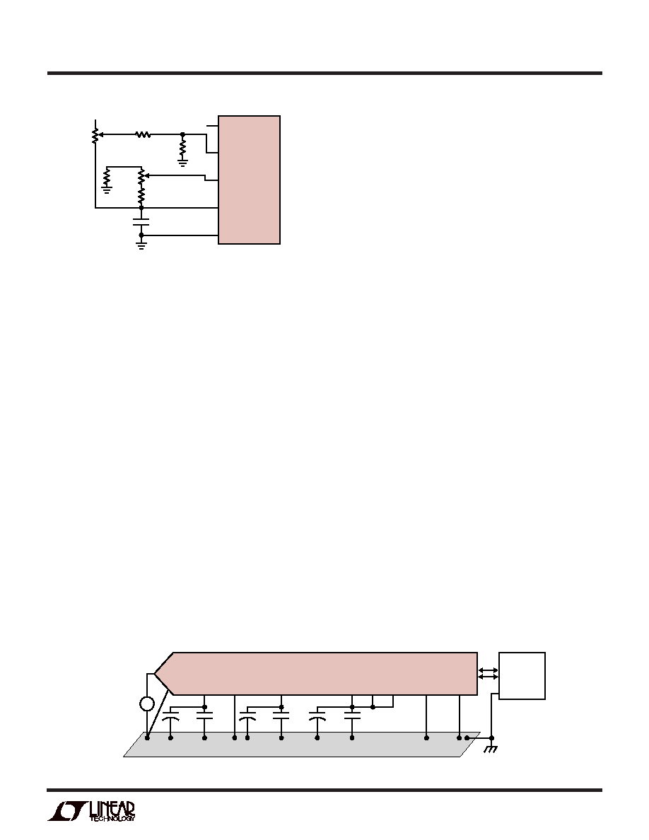
Figure 12. Power Supply Grounding Practice
LTC1412
AIN
+
ANALOG INPUT
AIN
–
VREF
REFCOMP
AGND
1412 F11b
1
2
3
R4
100
R2
50k
R3
24k
–5V
R6
24k
R1
50k
R5
47k
4
5
10
F
Figure 11b. Offset and Full-Scale Adjust Circuit
– 0.61mV (i.e., – 0.5LSB) at AIN+ and adjust the offset at
the AIN– input until the output code flickers between 0000
0000 0000 and 1111 1111 1111. For full-scale adjust-
ment, an input voltage of 2.49817V (FS/2 – 1.5LSBs) is
applied to AIN+ and R2 is adjusted until the output code
flickers between 0111 1111 1110 and 0111 1111 1111.
Board Layout and Bypassing
To obtain the best performance from the LTC1412, a
printed circuit board with ground plane is required. Layout
for the printed circuit board should ensure that digital and
analog signal lines are separated as much as possible. In
particular, care should be taken not to run any digital line
alongside an analog signal line.
An analog ground plane separate from the logic system
ground should be established under and around the ADC.
Pin 5 (AGND), Pins 19 and 14 (DGND) and Pin 22 (OGND)
and all other analog grounds should be connected to this
single analog ground point. The REFCOMP bypass capaci-
tor and the DVDD bypass capacitor should also be con-
nected to this analog ground plane, see Figure 12. All
analog circuitry grounds should be terminated to this
analog ground plane. The ground return from the ground
1412 F12
AIN
+
AGND
REFCOMP
VSS
AVDD
LTC1412
DIGITAL
SYSTEM
ANALOG
INPUT
CIRCUITRY
5
4
2
26
OVDD DVDD
21
20, 27
28
OGND
DGND
14, 19
22
POWER
SUPPLY
GROUND
1
0.1
F
AIN
–
0.1
F0.1F
10
F
ANALOG GROUND PLANE
+
–
+
10
F
10
F
+
相关PDF资料 |
PDF描述 |
|---|---|
| SP490EN-L/TR | IC TXRX RS485 FULL DUPLEX 8NSOIC |
| LTC1418AIN | IC A/D CONV 14BIT SRL&PAR 28-DIP |
| SP481ECN-L/TR | IC TXRX RS484 HALF DUPLEX 8NSOIC |
| MS27474E14B35P | CONN RCPT 37POS JAM NUT W/PINS |
| AD7895BRZ-2 | IC ADC 12BIT SRL 5V 8SOIC |
相关代理商/技术参数 |
参数描述 |
|---|---|
| LTC1412IG#PBF | 功能描述:IC A/D CONV 12BIT SAMPLNG 28SSOP RoHS:是 类别:集成电路 (IC) >> 数据采集 - 模数转换器 系列:- 标准包装:1,000 系列:- 位数:12 采样率(每秒):300k 数据接口:并联 转换器数目:1 功率耗散(最大):75mW 电压电源:单电源 工作温度:0°C ~ 70°C 安装类型:表面贴装 封装/外壳:24-SOIC(0.295",7.50mm 宽) 供应商设备封装:24-SOIC 包装:带卷 (TR) 输入数目和类型:1 个单端,单极;1 个单端,双极 |
| LTC1412IG#TR | 功能描述:IC ADC 12BIT 3MSPS SAMPLE 28SSOP RoHS:否 类别:集成电路 (IC) >> 数据采集 - 模数转换器 系列:- 标准包装:1,000 系列:- 位数:12 采样率(每秒):300k 数据接口:并联 转换器数目:1 功率耗散(最大):75mW 电压电源:单电源 工作温度:0°C ~ 70°C 安装类型:表面贴装 封装/外壳:24-SOIC(0.295",7.50mm 宽) 供应商设备封装:24-SOIC 包装:带卷 (TR) 输入数目和类型:1 个单端,单极;1 个单端,双极 |
| LTC1412IG#TRPBF | 功能描述:IC A/D CONV 12BIT SAMPLNG 28SSOP RoHS:是 类别:集成电路 (IC) >> 数据采集 - 模数转换器 系列:- 标准包装:1,000 系列:- 位数:12 采样率(每秒):300k 数据接口:并联 转换器数目:1 功率耗散(最大):75mW 电压电源:单电源 工作温度:0°C ~ 70°C 安装类型:表面贴装 封装/外壳:24-SOIC(0.295",7.50mm 宽) 供应商设备封装:24-SOIC 包装:带卷 (TR) 输入数目和类型:1 个单端,单极;1 个单端,双极 |
| LTC1414CGN | 功能描述:IC A/D CONV 14BIT SAMPLNG 28SSOP RoHS:否 类别:集成电路 (IC) >> 数据采集 - 模数转换器 系列:- 标准包装:1,000 系列:- 位数:12 采样率(每秒):300k 数据接口:并联 转换器数目:1 功率耗散(最大):75mW 电压电源:单电源 工作温度:0°C ~ 70°C 安装类型:表面贴装 封装/外壳:24-SOIC(0.295",7.50mm 宽) 供应商设备封装:24-SOIC 包装:带卷 (TR) 输入数目和类型:1 个单端,单极;1 个单端,双极 |
| LTC1414CGN#PBF | 功能描述:IC A/D CONV 14BIT SAMPLNG 28SSOP RoHS:是 类别:集成电路 (IC) >> 数据采集 - 模数转换器 系列:- 标准包装:1 系列:microPOWER™ 位数:8 采样率(每秒):1M 数据接口:串行,SPI? 转换器数目:1 功率耗散(最大):- 电压电源:模拟和数字 工作温度:-40°C ~ 125°C 安装类型:表面贴装 封装/外壳:24-VFQFN 裸露焊盘 供应商设备封装:24-VQFN 裸露焊盘(4x4) 包装:Digi-Reel® 输入数目和类型:8 个单端,单极 产品目录页面:892 (CN2011-ZH PDF) 其它名称:296-25851-6 |
发布紧急采购,3分钟左右您将得到回复。