- 您现在的位置:买卖IC网 > PDF目录10667 > LTC1418CG#PBF (Linear Technology)IC A/D CONV 14BIT SRL&PAR 28SSOP PDF资料下载
参数资料
| 型号: | LTC1418CG#PBF |
| 厂商: | Linear Technology |
| 文件页数: | 6/28页 |
| 文件大小: | 0K |
| 描述: | IC A/D CONV 14BIT SRL&PAR 28SSOP |
| 标准包装: | 47 |
| 位数: | 14 |
| 采样率(每秒): | 200k |
| 数据接口: | 串行,并联 |
| 转换器数目: | 1 |
| 功率耗散(最大): | 21.5mW 单极;31.5mW 双极 |
| 电压电源: | 双 ± |
| 工作温度: | 0°C ~ 70°C |
| 安装类型: | 表面贴装 |
| 封装/外壳: | 28-SSOP(0.209",5.30mm 宽) |
| 供应商设备封装: | 28-SSOP |
| 包装: | 管件 |
| 输入数目和类型: | 2 个单端,单极;2 个单端,双极;1 个差分,单极;1 个差分,双极 |
| 产品目录页面: | 1346 (CN2011-ZH PDF) |
| 配用: | DC178A-ND - BOARD SAR ADC LTC1418 |
第1页第2页第3页第4页第5页当前第6页第7页第8页第9页第10页第11页第12页第13页第14页第15页第16页第17页第18页第19页第20页第21页第22页第23页第24页第25页第26页第27页第28页
14
LTC1418
APPLICATIONS INFORMATION
WU
U
nected to this analog ground plane. Low impedance ana-
log and digital power supply common returns are essential
to low noise operation of the ADC and the foil width for
these tracks should be as wide as possible. In applications
where the ADC data outputs and control signals are
connected to a continuously active microprocessor bus, it
is possible to get errors in the conversion results. These
errors are due to feedthrough from the microprocessor to
the successive approximation comparator. The problem
can be eliminated by forcing the microprocessor into a
wait state during conversion or by using three-state buff-
ers to isolate the ADC data bus. The traces connecting the
pins and bypass capacitors must be kept short and should
be made as wide as possible.
The LTC1418 has differential inputs to minimize noise
coupling. Common mode noise on the AIN+ and AIN– leads
will be rejected by the input CMRR. The AIN– input can be
used as a ground sense for the AIN
+ input; the LTC1418 will
hold and convert the difference voltage between AIN+ and
AIN–. The leads to AIN+ (Pin 1) and AIN– (Pin 2) should be
kept as short as possible. In applications where this is not
possible, the AIN+ and AIN– traces should be run side by
side to equalize coupling.
SUPPLY BYPASSING
High quality, low series resistance ceramic, 10
F bypass
capacitors should be used at the VDD and REFCOMP pins.
Surface mount ceramic capacitors such as Murata
GRM235Y5V106Z016 provide excellent bypassing in a
small board space. Alternatively 10
F tantalum capacitors
in parallel with 0.1
F ceramic capacitors can be used.
error adjustment is achieved by adjusting the offset
applied to the AIN– input. For zero offset error apply
– 125
V (i.e., –0.5LSB) at AIN+ and adjust the offset
at the AIN
– input until the output code flickers between
0000 0000 0000 00 and 1111 1111 1111 11. For
full-scale adjustment, an input voltage of 2.047625V
(FS – 1.5LSBs) is applied to AIN
+ and R2 is adjusted until
the output code flickers between 0111 1111 1111 10 and
0111 1111 1111 11.
BOARD LAYOUT AND GROUNDING
Wire wrap boards are not recommended for high resolu-
tion or high speed A/D converters. To obtain the best
performance from the LTC1418, a printed circuit board
with ground plane is required. The ground plane under the
ADC area should be as free of breaks and holes as
possible, such that a low impedance path between all ADC
grounds and all ADC decoupling capacitors is provided. It
is critical to prevent digital noise from being coupled to the
analog input, reference or analog power supply lines.
Layout should ensure that digital and analog signal lines
are separated as much as possible. In particular, care
should be taken not to run any digital track alongside an
analog signal track.
An analog ground plane separate from the logic system
ground should be established under and around the ADC.
Pin 5 (AGND) and Pin 14 (DGND) and all other analog
grounds should be connected to this single analog ground
plane. The REFCOMP bypass capacitor and the VDD by-
pass capacitor should also be connected to this analog
ground plane. No other digital grounds should be con-
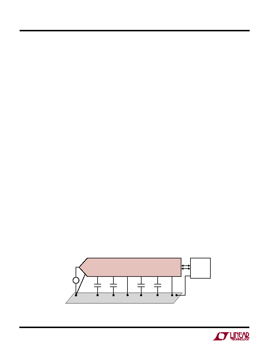
1418 F11
DIGITAL
SYSTEM
ANALOG
INPUT
CIRCUITRY
5
4
2
27
28
14
1
10
F
3
1
F10F
10
F
ANALOG GROUND PLANE
+
–
AIN
+
AGND
REFCOMP
VSS
VREF
VDD
LTC1418
DGND
AIN
–
Figure 11. Power Supply Grounding Practice
相关PDF资料 |
PDF描述 |
|---|---|
| AD7574JNZ | IC ADC 8BIT CMOS 5V 18-DIP |
| AD7767BRUZ | ADC 24BIT 128KSPS SAR 16-TSSOP |
| AD7660ASTZ | IC ADC 16BIT UNIPOLAR 48-LQFP |
| VE-J11-MW-F1 | CONVERTER MOD DC/DC 12V 100W |
| LTC1403AIMSE#PBF | IC ADC 14BIT 2.8MSPS 10-MSOP |
相关代理商/技术参数 |
参数描述 |
|---|---|
| LTC1418CN#PBF | 功能描述:IC A/D CONV 14BIT SRL&PAR 28-DIP RoHS:是 类别:集成电路 (IC) >> 数据采集 - 模数转换器 系列:- 标准包装:1,000 系列:- 位数:12 采样率(每秒):300k 数据接口:并联 转换器数目:1 功率耗散(最大):75mW 电压电源:单电源 工作温度:0°C ~ 70°C 安装类型:表面贴装 封装/外壳:24-SOIC(0.295",7.50mm 宽) 供应商设备封装:24-SOIC 包装:带卷 (TR) 输入数目和类型:1 个单端,单极;1 个单端,双极 |
| LTC1418IG | 功能描述:IC A/D CONV 14BIT SRL&PAR 28SSOP RoHS:否 类别:集成电路 (IC) >> 数据采集 - 模数转换器 系列:- 标准包装:1,000 系列:- 位数:12 采样率(每秒):300k 数据接口:并联 转换器数目:1 功率耗散(最大):75mW 电压电源:单电源 工作温度:0°C ~ 70°C 安装类型:表面贴装 封装/外壳:24-SOIC(0.295",7.50mm 宽) 供应商设备封装:24-SOIC 包装:带卷 (TR) 输入数目和类型:1 个单端,单极;1 个单端,双极 |
| LTC1418IG#PBF | 功能描述:IC A/D CONV 14BIT SRL&PAR 28SSOP RoHS:是 类别:集成电路 (IC) >> 数据采集 - 模数转换器 系列:- 标准包装:1,000 系列:- 位数:12 采样率(每秒):300k 数据接口:并联 转换器数目:1 功率耗散(最大):75mW 电压电源:单电源 工作温度:0°C ~ 70°C 安装类型:表面贴装 封装/外壳:24-SOIC(0.295",7.50mm 宽) 供应商设备封装:24-SOIC 包装:带卷 (TR) 输入数目和类型:1 个单端,单极;1 个单端,双极 |
| LTC1418IG#TR | 功能描述:IC A/D CONV 14BIT SRL&PAR 28SSOP RoHS:否 类别:集成电路 (IC) >> 数据采集 - 模数转换器 系列:- 标准包装:1,000 系列:- 位数:12 采样率(每秒):300k 数据接口:并联 转换器数目:1 功率耗散(最大):75mW 电压电源:单电源 工作温度:0°C ~ 70°C 安装类型:表面贴装 封装/外壳:24-SOIC(0.295",7.50mm 宽) 供应商设备封装:24-SOIC 包装:带卷 (TR) 输入数目和类型:1 个单端,单极;1 个单端,双极 |
| LTC1418IG#TRPBF | 功能描述:IC A/D CONV 14BIT SRL&PAR 28SSOP RoHS:是 类别:集成电路 (IC) >> 数据采集 - 模数转换器 系列:- 标准包装:1,000 系列:- 位数:12 采样率(每秒):300k 数据接口:并联 转换器数目:1 功率耗散(最大):75mW 电压电源:单电源 工作温度:0°C ~ 70°C 安装类型:表面贴装 封装/外壳:24-SOIC(0.295",7.50mm 宽) 供应商设备封装:24-SOIC 包装:带卷 (TR) 输入数目和类型:1 个单端,单极;1 个单端,双极 |
发布紧急采购,3分钟左右您将得到回复。