- 您现在的位置:买卖IC网 > PDF目录10175 > LTC1419ISW#TR (Linear Technology)IC ADC 14BIT 800KSPS SHDN 28SOIC PDF资料下载
参数资料
| 型号: | LTC1419ISW#TR |
| 厂商: | Linear Technology |
| 文件页数: | 5/20页 |
| 文件大小: | 0K |
| 描述: | IC ADC 14BIT 800KSPS SHDN 28SOIC |
| 标准包装: | 1,000 |
| 位数: | 14 |
| 采样率(每秒): | 800k |
| 数据接口: | 并联 |
| 转换器数目: | 1 |
| 功率耗散(最大): | 240mW |
| 电压电源: | 双 ± |
| 工作温度: | -40°C ~ 85°C |
| 安装类型: | 表面贴装 |
| 封装/外壳: | 28-SOIC(0.295",7.50mm 宽) |
| 供应商设备封装: | 28-SOIC |
| 包装: | 带卷 (TR) |
| 输入数目和类型: | 2 个单端,双极;1 个差分,双极 |
13
LTC1419
1419fb
APPLICATIONS INFORMATION
WU
U
applied to the – AIN input. For zero offset error, apply
– 152
V (i.e., –0.5LSB) at +AIN and adjust the offset at the
–AIN input until the output code flickers between 0000
0000 0000 00 and 1111 1111 1111 11. For full-scale
adjustment, an input voltage of 2.499544V (FS/2 – 1.5LSBs)
is applied to + AIN and R2 is adjusted until
the output code flickers between 0111 1111 1111 10 and
0111 1111 1111 11.
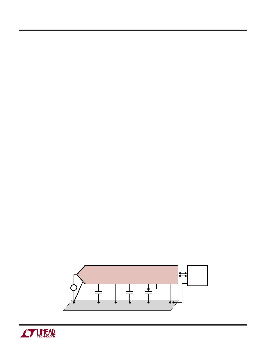
BOARD LAYOUT AND GROUNDING
Wire wrap boards are not recommended for high resolu-
tion or high speed A/D converters. To obtain the best
performance from the LTC1419, a printed circuit board
with ground plane is required. Layout should ensure that
digital and analog signal lines are separated as much as
possible. Particular care should be taken not to run any
digital track alongside an analog signal track or under-
neath the ADC.The analog input should be screened by
AGND.
An analog ground plane separate from the logic system
ground should be established under and around the ADC.
Pin 5 (AGND), Pin 14 and Pin 19 (ADC’s DGND) and all
other analog grounds should be connected to this single
analog ground point. The REFCOMP bypass capacitor and
the DVDD bypass capacitor should also be connected to
this analog ground plane. No other digital grounds should
be connected to this analog ground plane. Low impedance
analog and digital power supply common returns are
essential to low noise operation of the ADC and the foil
width for these tracks should be as wide as possible. In
applications where the ADC data outputs and control
signals are connected to a continuously active micropro-
cessor bus, it is possible to get errors in the conversion
results. These errors are due to feedthrough from the
microprocessor to the successive approximation com-
parator. The problem can be eliminated by forcing the
microprocessor into a WAIT state during conversion or by
using three-state buffers to isolate the ADC data bus. The
traces connecting the pins and bypass capacitors must be
kept short and should be made as wide as possible.
The LTC1419 has differential inputs to minimize noise
coupling. Common mode noise on the + AIN and –AIN
leads will be rejected by the input CMRR. The – AIN input
can be used as a ground sense for the + AIN input; the
LTC1419 will hold and convert the difference voltage
between + AIN and –AIN. The leads to + AIN (Pin 1) and –AIN
(Pin 2) should be kept as short as possible. In applications
where this is not possible, the + AIN and –AIN traces should
be run side by side to equalize coupling.
SUPPLY BYPASSING
High quality, low series resistance ceramic, 10
F bypass
capacitors should be used at the VDD and REFCOMP pins
as shown in the Typical Application on the fist page of this
data sheet. Surface mount ceramic capacitors such as
Murata GRM235Y5V106Z016 provide excellent bypass-
ing in a small board space. Alternatively, 10
F tantalum
capacitors in parallel with 0.1
F ceramic capacitors can be
used. Bypass capacitors must be located as close to the
pins as possible. The traces connecting the pins and the
bypass capacitors must be kept short and should be made
as wide as possible.
Example Layout
Figures 13a, 13b, 13c and 13d show the schematic and
layout of a suggested evaluation board. The layout demon-
strates the proper use of decoupling capacitors and ground
plane with a 2-layer printed circuit board.
Figure 12. Power Supply Grounding Practice
1419 F12
+AIN
AGND
REFCOMP
VSS
AVDD
LTC1419
DIGITAL
SYSTEM
ANALOG
INPUT
CIRCUITRY
5
4
2
26
28
DVDD
27
DGND
14
1
10
F
–AIN
10
F
10
F
ANALOG GROUND PLANE
+
–
相关PDF资料 |
PDF描述 |
|---|---|
| VE-26W-CU-F2 | CONVERTER MOD DC/DC 5.5V 200W |
| CXC3102A2029S | CONN RCPT 17POS PNL MNT SKT |
| VE-JTN-MX-S | CONVERTER MOD DC/DC 18.5V 75W |
| IDT72V2113L6PFG | IC FIFO SUPERSYNCII 6NS 80TQFP |
| ADM211ARZ-REEL | IC TXRX RS-232 5V 0.1UF 28SOIC |
相关代理商/技术参数 |
参数描述 |
|---|---|
| LTC1420CGN | 功能描述:IC ADC 12BIT 10MSPS SAMPL 28SSOP RoHS:否 类别:集成电路 (IC) >> 数据采集 - 模数转换器 系列:- 标准包装:1,000 系列:- 位数:16 采样率(每秒):45k 数据接口:串行 转换器数目:2 功率耗散(最大):315mW 电压电源:模拟和数字 工作温度:0°C ~ 70°C 安装类型:表面贴装 封装/外壳:28-SOIC(0.295",7.50mm 宽) 供应商设备封装:28-SOIC W 包装:带卷 (TR) 输入数目和类型:2 个单端,单极 |
| LTC1420CGN#PBF | 功能描述:IC ADC 12BIT 10MSPS SAMPL 28SSOP RoHS:是 类别:集成电路 (IC) >> 数据采集 - 模数转换器 系列:- 标准包装:1 系列:microPOWER™ 位数:8 采样率(每秒):1M 数据接口:串行,SPI? 转换器数目:1 功率耗散(最大):- 电压电源:模拟和数字 工作温度:-40°C ~ 125°C 安装类型:表面贴装 封装/外壳:24-VFQFN 裸露焊盘 供应商设备封装:24-VQFN 裸露焊盘(4x4) 包装:Digi-Reel® 输入数目和类型:8 个单端,单极 产品目录页面:892 (CN2011-ZH PDF) 其它名称:296-25851-6 |
| LTC1420CGN#PBF | 制造商:Linear Technology 功能描述:ADC, 12BIT, 10MSPS, SSOP-28 |
| LTC1420CGN#TR | 功能描述:IC ADC 12BIT 10MSPS SAMPL 28SSOP RoHS:否 类别:集成电路 (IC) >> 数据采集 - 模数转换器 系列:- 标准包装:1,000 系列:- 位数:16 采样率(每秒):45k 数据接口:串行 转换器数目:2 功率耗散(最大):315mW 电压电源:模拟和数字 工作温度:0°C ~ 70°C 安装类型:表面贴装 封装/外壳:28-SOIC(0.295",7.50mm 宽) 供应商设备封装:28-SOIC W 包装:带卷 (TR) 输入数目和类型:2 个单端,单极 |
| LTC1420CGN#TRPBF | 功能描述:IC ADC 12BIT 10MSPS SAMPL 28SSOP RoHS:是 类别:集成电路 (IC) >> 数据采集 - 模数转换器 系列:- 标准包装:1,000 系列:- 位数:16 采样率(每秒):45k 数据接口:串行 转换器数目:2 功率耗散(最大):315mW 电压电源:模拟和数字 工作温度:0°C ~ 70°C 安装类型:表面贴装 封装/外壳:28-SOIC(0.295",7.50mm 宽) 供应商设备封装:28-SOIC W 包装:带卷 (TR) 输入数目和类型:2 个单端,单极 |
发布紧急采购,3分钟左右您将得到回复。