- 您现在的位置:买卖IC网 > PDF目录10296 > LTC1420CGN (Linear Technology)IC ADC 12BIT 10MSPS SAMPL 28SSOP PDF资料下载
参数资料
| 型号: | LTC1420CGN |
| 厂商: | Linear Technology |
| 文件页数: | 4/20页 |
| 文件大小: | 0K |
| 描述: | IC ADC 12BIT 10MSPS SAMPL 28SSOP |
| 标准包装: | 49 |
| 位数: | 12 |
| 采样率(每秒): | 10M |
| 数据接口: | 并联 |
| 转换器数目: | 1 |
| 功率耗散(最大): | 300mW |
| 电压电源: | 单电源 |
| 工作温度: | 0°C ~ 70°C |
| 安装类型: | 表面贴装 |
| 封装/外壳: | 28-SSOP(0.154",3.90mm 宽) |
| 供应商设备封装: | 28-SSOP |
| 包装: | 管件 |
| 输入数目和类型: | 2 个单端,双极;1 个差分,双极 |
12
LTC1420
1420fa
INPUT VOLTAGE (V)
–(FS – 1LSB)
FS – 1LSB
OUTPUT
CODE
1420 F10
011…111
011…110
011…101
100…010
100…001
100…000
OVERFLOW
BIT
1
0
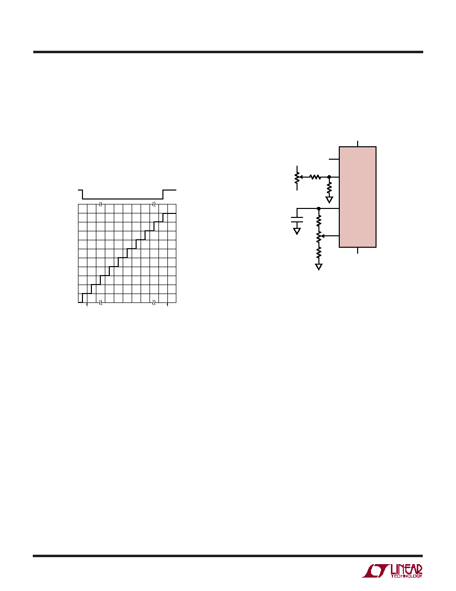
Figure 10. LTC1420 Transfer Characteristics
R2
1k
10k
1F
1420 F11
+AIN
VSS
VIN
5V
–5V
LTC1420
5V
–AIN
SENSE
VREF
10k
24k
100
R1
50k
Figure 11. Offset and Full-Scale Adjust Circuit
APPLICATIONS INFORMATION
WU
U
Digital Outputs and Overflow Bit (OF)
Figure 10 shows the ideal input/output characteristics for
the LTC1420. The output data is two’s complement binary
for all input ranges and for both single and dual supply
operation. One LSB = VREF/4096. To create a straight
binary output, invert the MSB (D11). The overflow bit (OF)
indicates when the analog input is outside the input range
of the converter. OF is high when the output code is 1000
0000 0000 or 0111 1111 1111.
Full-Scale and Offset Adjustment
In applications where absolute accuracy is important,
offset and full-scale errors can be adjusted to zero. Offset
error should be adjusted before full-scale error. Figure 11
shows a method for error adjustment for a dual supply,
4.096V application. For zero offset error apply – 0.5mV
(i. e., – 0.5LSB) at + AIN and adjust R1 until the output code
flickers between 0000 0000 0000 and 1111 1111 1111.
For full-scale adjustment, apply an input voltage of 2.0465V
(FS – 1.5LSBs) at + AIN and adjust R2 until the output code
flickers between 0111 1111 1110 and 0111 1111 1111.
Digital Output Drivers
The LTC1420 output drivers can interface to logic operat-
ing from 3V to 5V by setting OVDD to the logic power
supply. If 5V output is desired, OVDD can be shorted to VDD
and share its decoupling capacitor. Otherwise, OVDD re-
quires its own 1F decoupling capacitor. To prevent digital
noise from affecting performance, the load capacitance on
the digital outputs should be minimized. If large capacitive
loads are required (>30pF), external buffers or 100
resistors in series with the digital outputs are suggested.
Timing
The conversion start is controlled by the rising edge of the
CLK pin. Once a conversion is started, it cannot be stopped
or restarted until the conversion cycle is complete. Output
data is updated at the end of conversion, or about 70ns
after a conversion is begun. There is an additional two
cycle pipeline delay, so the data for a given conversion is
output two full clock cycles plus 70ns after the convert
start. Thus, output data can be latched on the third CLK
rising edge after the rising edge that samples the input.
Clock Input
The LTC1420 only uses the rising edge of the CLK pin for
internal timing, and CLK doesn’t necessarily need to have
a 50% duty cycle. For optimal AC performance, the rise
time of the CLK should be less than 5ns. If the available
clock has a rise time slower than 5ns, it can be locally sped
up with a logic gate. With single supply operation, the
clock can be driven with 5V CMOS, 3V CMOS or TTL logic
levels. With dual power supplies, the clock should be
driven with 5V CMOS levels.
As with all fast ADCs, the noise performance of the
LTC1420 is sensitive to clock jitter when high speed inputs
相关PDF资料 |
PDF描述 |
|---|---|
| D38999/20WG11SNLC | CONN HSG RCPT 11POS WALL MT SCKT |
| LTC1405CGN | IC ADC 12BIT 5MSPS SAMPLE 28SSOP |
| VE-B6P-IW-B1 | CONVERTER MOD DC/DC 13.8V 100W |
| LTC2366CTS8#TRPBF | IC ADC 12BIT 3MSPS TSOT23-8 |
| VE-B6N-IX-B1 | CONVERTER MOD DC/DC 18.5V 75W |
相关代理商/技术参数 |
参数描述 |
|---|---|
| LTC1420CGN#PBF | 功能描述:IC ADC 12BIT 10MSPS SAMPL 28SSOP RoHS:是 类别:集成电路 (IC) >> 数据采集 - 模数转换器 系列:- 标准包装:1 系列:microPOWER™ 位数:8 采样率(每秒):1M 数据接口:串行,SPI? 转换器数目:1 功率耗散(最大):- 电压电源:模拟和数字 工作温度:-40°C ~ 125°C 安装类型:表面贴装 封装/外壳:24-VFQFN 裸露焊盘 供应商设备封装:24-VQFN 裸露焊盘(4x4) 包装:Digi-Reel® 输入数目和类型:8 个单端,单极 产品目录页面:892 (CN2011-ZH PDF) 其它名称:296-25851-6 |
| LTC1420CGN#PBF | 制造商:Linear Technology 功能描述:ADC, 12BIT, 10MSPS, SSOP-28 |
| LTC1420CGN#TR | 功能描述:IC ADC 12BIT 10MSPS SAMPL 28SSOP RoHS:否 类别:集成电路 (IC) >> 数据采集 - 模数转换器 系列:- 标准包装:1,000 系列:- 位数:16 采样率(每秒):45k 数据接口:串行 转换器数目:2 功率耗散(最大):315mW 电压电源:模拟和数字 工作温度:0°C ~ 70°C 安装类型:表面贴装 封装/外壳:28-SOIC(0.295",7.50mm 宽) 供应商设备封装:28-SOIC W 包装:带卷 (TR) 输入数目和类型:2 个单端,单极 |
| LTC1420CGN#TRPBF | 功能描述:IC ADC 12BIT 10MSPS SAMPL 28SSOP RoHS:是 类别:集成电路 (IC) >> 数据采集 - 模数转换器 系列:- 标准包装:1,000 系列:- 位数:16 采样率(每秒):45k 数据接口:串行 转换器数目:2 功率耗散(最大):315mW 电压电源:模拟和数字 工作温度:0°C ~ 70°C 安装类型:表面贴装 封装/外壳:28-SOIC(0.295",7.50mm 宽) 供应商设备封装:28-SOIC W 包装:带卷 (TR) 输入数目和类型:2 个单端,单极 |
| LTC1420IGN | 功能描述:IC ADC 12BIT 10MSPS SAMPL 28SSOP RoHS:否 类别:集成电路 (IC) >> 数据采集 - 模数转换器 系列:- 标准包装:1,000 系列:- 位数:16 采样率(每秒):45k 数据接口:串行 转换器数目:2 功率耗散(最大):315mW 电压电源:模拟和数字 工作温度:0°C ~ 70°C 安装类型:表面贴装 封装/外壳:28-SOIC(0.295",7.50mm 宽) 供应商设备封装:28-SOIC W 包装:带卷 (TR) 输入数目和类型:2 个单端,单极 |
发布紧急采购,3分钟左右您将得到回复。