- 您现在的位置:买卖IC网 > PDF目录20041 > LTC1422IS8#PBF (Linear Technology)IC CONTROLLER HOT SWAP 8-SOIC PDF资料下载
参数资料
| 型号: | LTC1422IS8#PBF |
| 厂商: | Linear Technology |
| 文件页数: | 10/16页 |
| 文件大小: | 197K |
| 描述: | IC CONTROLLER HOT SWAP 8-SOIC |
| 标准包装: | 100 |
| 类型: | 热交换控制器 |
| 应用: | 通用 |
| 内部开关: | 无 |
| 电源电压: | 2.7 V ~ 12 V |
| 工作温度: | -40°C ~ 85°C |
| 安装类型: | 表面贴装 |
| 封装/外壳: | 8-SOIC(0.154",3.90mm 宽) |
| 供应商设备封装: | 8-SOIC |
| 包装: | 管件 |
| 产品目录页面: | 1341 (CN2011-ZH PDF) |
10
LTC1422
1422fb
1
2
3
4
8
7
6
5
V
CC
SENSE
GATE
FB
RESET
ON
TIMER
GND
LTC1422
1422 F10
D1
1N4148
Q1
1/2 Si9436
Q2
1/2 Si99436
R2
0.01&
5%
R3
10&
5%
C1
0.33礔
16V
R1
10k
5%
RESET
ON
R6
1M
5%
R7
10&
5%
R4
2.74k
1%
TRIP POINT: 4.6V
R5
1k
1%
C3
0.047礔
25V
C2
0.022礔
25V
C
LOAD
C
LOAD
V
OUT
3.3V
V
OUT
5V
V
IN
3.3V
V
IN
5V
5V OUT
3.3V OUT
CURRENT LIMIT: 5A
+
+
Figure 10. Switching 5V and 3.3V
+
SENSE
R4
R3
R2
7
V
CC
V
OUT
V
CC
8
10k
GATE
LTC1422
6
2
REF
FB
1422 F09
1
5
C2
Q2: 2N7002LT1
Q3, Q4: MMBT3904LT1
Q2
ON/RESET
3
TIMER
ON
4
RESET
C1
C
LOAD
Q1
R1
LOGIC
+
COMP 5
10k
10k
Q3
Q4
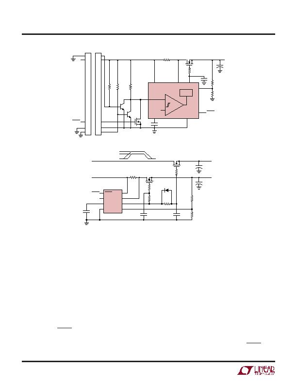
Figure 9. ON Pin Circuitry
and C3 are used to set the rise and fall delays on the 5V
supply. Next, the 3.3V supply ramps up with a 20ms delay
set by R6 and C2. On the falling edge, the 3.3V supply
ramps down first because R6 is bypassed by the diode D1.
Using the LTC1422 as a Linear Regulator
The LTC1422 can be used to Hot Swap the primary supply
and generate a secondary low dropout regulated supply.
Figure 11 shows how to switch a 5V supply and create a
3.3V supply using the reset comparator and one addi-
tional transistor. The FB pin is used to monitor the 3.3V
output. When the voltage on the gate of Q2 increases, the
3.3V increases. At the 3.3V threshold, the reset compara-
tor will trip. The RESET pin goes high which turns on Q3.
This lowers the voltage on the gate of Q2. This feedback
loop is compensated by the capacitor C1 and the resistors
R6 and R7.
Hot Swapping 48V DC/DC Module with
Active Low On/Off Control Signal
Using a 7.5V Zener and a resistor, the LTC1422 can switch
supplies much greater than the 12V V
CC
pin rating. As
shown in Figure 12, the switching FET Q1 is connected as
a common source driver rather than the usual source
follower used in previous applications. This allows the
ground of the LTC1422 to sit at the negative terminal of the
48V input. The clamp circuit of R5 and D1 provides power
to the LTC1422. The resistive divider R1 and R2 at the ON
pin monitors the input supply. The switching FET Q1 is
prevented from turning on until the input supply is at least
38V. Using the reset comparator to monitor the gate
voltage allows the module to be turned on after the gate
has reached a minimum level plus one timing cycle. A high
voltage transistor Q2 is used to translate the RESET signal
to the module On/Off input.
APPLICATIONS INFORMATION
U
U
U
相关PDF资料 |
PDF描述 |
|---|---|
| NCP694HSANADJT1G | IC REG LDO ADJ 1A 6HSON |
| EMA49DRMN-S288 | CONN EDGECARD 98POS .125 EXTEND |
| 3-338309-2 | CONN D-SUB PLUG VERT 9POS |
| CENT1120A1551F01 | PS EXT 110W 15V @ 7.33A E-STAR |
| CDRR75NP-150MC | INDUCTOR POWER 15UH 2.07A SMD |
相关代理商/技术参数 |
参数描述 |
|---|---|
| LTC1426CMS8 | 功能描述:IC PWM D/A CONV 6BIT DUAL 8-MSOP RoHS:否 类别:集成电路 (IC) >> 数据采集 - 数模转换器 系列:- 产品培训模块:LTC263x 12-, 10-, and 8-Bit VOUT DAC Family 特色产品:LTC2636 - Octal 12-/10-/8-Bit SPI VOUT DACs with 10ppm/°C Reference 标准包装:91 系列:- 设置时间:4µs 位数:10 数据接口:MICROWIRE?,串行,SPI? 转换器数目:8 电压电源:单电源 功率耗散(最大):2.7mW 工作温度:-40°C ~ 85°C 安装类型:表面贴装 封装/外壳:14-WFDFN 裸露焊盘 供应商设备封装:14-DFN-EP(4x3) 包装:管件 输出数目和类型:8 电压,单极 采样率(每秒):* |
| LTC1426CMS8#PBF | 功能描述:IC PWM D/A CONV 6BIT DUAL 8-MSOP RoHS:是 类别:集成电路 (IC) >> 数据采集 - 数模转换器 系列:- 标准包装:2,400 系列:- 设置时间:- 位数:18 数据接口:串行 转换器数目:3 电压电源:模拟和数字 功率耗散(最大):- 工作温度:-40°C ~ 85°C 安装类型:表面贴装 封装/外壳:36-TFBGA 供应商设备封装:36-TFBGA 包装:带卷 (TR) 输出数目和类型:* 采样率(每秒):* |
| LTC1426CMS8#TR | 功能描述:IC DAC PWM 6BIT DUAL MCPWR 8MSOP RoHS:否 类别:集成电路 (IC) >> 数据采集 - 数模转换器 系列:- 产品培训模块:LTC263x 12-, 10-, and 8-Bit VOUT DAC Family 特色产品:LTC2636 - Octal 12-/10-/8-Bit SPI VOUT DACs with 10ppm/°C Reference 标准包装:91 系列:- 设置时间:4µs 位数:10 数据接口:MICROWIRE?,串行,SPI? 转换器数目:8 电压电源:单电源 功率耗散(最大):2.7mW 工作温度:-40°C ~ 85°C 安装类型:表面贴装 封装/外壳:14-WFDFN 裸露焊盘 供应商设备封装:14-DFN-EP(4x3) 包装:管件 输出数目和类型:8 电压,单极 采样率(每秒):* |
| LTC1426CMS8#TRPBF | 功能描述:IC PWM D/A CONV 6BIT DUAL 8-MSOP RoHS:是 类别:集成电路 (IC) >> 数据采集 - 数模转换器 系列:- 标准包装:2,400 系列:- 设置时间:- 位数:18 数据接口:串行 转换器数目:3 电压电源:模拟和数字 功率耗散(最大):- 工作温度:-40°C ~ 85°C 安装类型:表面贴装 封装/外壳:36-TFBGA 供应商设备封装:36-TFBGA 包装:带卷 (TR) 输出数目和类型:* 采样率(每秒):* |
| LTC1426CS8 | 功能描述:IC PWM D/A CONV 6BIT DUAL 8-SOIC RoHS:否 类别:集成电路 (IC) >> 数据采集 - 数模转换器 系列:- 产品培训模块:LTC263x 12-, 10-, and 8-Bit VOUT DAC Family 特色产品:LTC2636 - Octal 12-/10-/8-Bit SPI VOUT DACs with 10ppm/°C Reference 标准包装:91 系列:- 设置时间:4µs 位数:10 数据接口:MICROWIRE?,串行,SPI? 转换器数目:8 电压电源:单电源 功率耗散(最大):2.7mW 工作温度:-40°C ~ 85°C 安装类型:表面贴装 封装/外壳:14-WFDFN 裸露焊盘 供应商设备封装:14-DFN-EP(4x3) 包装:管件 输出数目和类型:8 电压,单极 采样率(每秒):* |
发布紧急采购,3分钟左右您将得到回复。