- 您现在的位置:买卖IC网 > PDF目录224113 > LTC1422IS8#PBF (LINEAR TECHNOLOGY CORP) Hot Swap Controller; Package: SO; No of Pins: 8; Temperature Range: -40°C to +85°C PDF资料下载
参数资料
| 型号: | LTC1422IS8#PBF |
| 厂商: | LINEAR TECHNOLOGY CORP |
| 元件分类: | 电源管理 |
| 英文描述: | Hot Swap Controller; Package: SO; No of Pins: 8; Temperature Range: -40°C to +85°C |
| 中文描述: | 1-CHANNEL POWER SUPPLY SUPPORT CKT, PDSO8 |
| 封装: | 0.150 INCH, PLASTIC, SO-8 |
| 文件页数: | 16/16页 |
| 文件大小: | 193K |
| 代理商: | LTC1422IS8#PBF |
9
LTC1422
1422fb
APPLICATIONS INFORMATION
WU
U
When the timer is off, the internal N-channel Q1 shorts the
TIMER pin to ground. When the timer is turned on, a 2
A
current from VCC is connected to the TIMER pin and the
voltage on the external capacitor C2 starts to ramp up with
a slope given by: dV/dt = 2
A/C2. When the voltage
reaches the trip point (1.232V), the timer will be reset by
pulling the TIMER pin back to ground. The timer period is
given by: (1.232V C2)/2
A. For a 200ms delay, use a
0.33
F capacitor.
Electronic Circuit Breaker
The LTC1422 features an electronic circuit breaker func-
tion that protects against short circuits or excessive cur-
rents on the supply. By placing a sense resistor between
the supply input and SENSE pin, the circuit breaker will be
tripped whenever the voltage across the sense resistor is
greater than 50mV for more than 10
s. When the circuit
breaker trips, the GATE pin is immediately pulled to
ground and the external N-channel is quickly turned off.
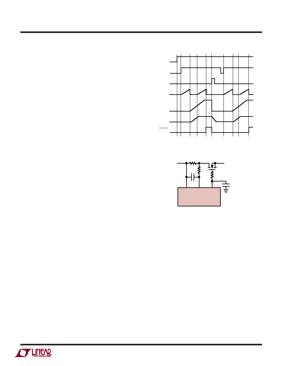
When the ON pin is cycled off for greater than 40
s and
then on as shown in Figure 7, time point 7, the circuit
breaker is reset and another timing cycle is started.
At the end of the timer cycle (time point 8), the charge
pump will turn on again. If the circuit breaker feature is not
required, the SENSE pin should be shorted to VCC.
If more than 10
s of response time is needed to reject
supply noise, an external resistor and capacitor can be
added to the sense circuit as shown in Figure 8.
Connection Sense with ON Pin
The ON pin can be used to sense board connection to the
backplane as shown in Figure 9.
Using staggered connection pins, ground mates first to
discharge any static build up on the board, followed by the
VCC connection and all other pins. When VCC makes
connection, the bases of transistors Q3 and Q4 are pulled
high turning them on and pulling the ON pin to ground.
When the base connector pins of Q3 and Q4 finally mate
to the backplane, the bases are shorted to ground. This
turns off Q3 and Q4 and allows the ON pin to pull high and
start a power-up cycle. The base connection pins of Q3 and
Q4 should be located at opposite ends of the connector
RESET
VOUT
GATE
1422 F07
TIMER
ON
VCC – VSENSE
VCC
1 2
3
4
5
6
7
8
9
10
because most people will rock the board back and forth to
get it seated properly.
A software-initiated power-down cycle can be started by
momentarily turning on transistor Q2, which will pull the
ON pin to ground. If the ON pin is held low for greater than
40
s, the GATE pin is pulled to ground. If the low pulse on
the ON pin is less than 15
s, a soft reset is generated.
Hot Swapping Two Supplies
With two external pass transistors, the LTC1422 can
switch two supplies. In some cases, it is necessary to bring
up the dominant supply first during power-up and ramp it
down last during the power-down phase. The circuit in
Figure 10 shows how to program two different delays for
the pass transistors. The 5V supply is powered up first. R1
Figure 7. Current Fault Timing
SENSE
7
VCC
8
GATE
LTC1422
6
C1
1422 F08
Q1
R1
RF
CF
R2
Figure 8. Extending the Short-Circuit Protection Delay
相关PDF资料 |
PDF描述 |
|---|---|
| LTC1422IS8#TRPBF | Hot Swap Controller; Package: SO; No of Pins: 8; Temperature Range: -40°C to +85°C |
| LTC1426CMS8#PBF | Micropower Dual 6-Bit PWM DAC; Package: MSOP; No of Pins: 8; Temperature Range: 0°C to +70°C |
| LTC1426CMS8#TRPBF | Micropower Dual 6-Bit PWM DAC; Package: MSOP; No of Pins: 8; Temperature Range: 0°C to +70°C |
| LTC1426CS8#PBF | Micropower Dual 6-Bit PWM DAC; Package: SO; No of Pins: 8; Temperature Range: 0°C to +70°C |
| LTC1426CS8#TRPBF | Micropower Dual 6-Bit PWM DAC; Package: SO; No of Pins: 8; Temperature Range: 0°C to +70°C |
相关代理商/技术参数 |
参数描述 |
|---|---|
| LTC1426CMS8 | 功能描述:IC PWM D/A CONV 6BIT DUAL 8-MSOP RoHS:否 类别:集成电路 (IC) >> 数据采集 - 数模转换器 系列:- 产品培训模块:LTC263x 12-, 10-, and 8-Bit VOUT DAC Family 特色产品:LTC2636 - Octal 12-/10-/8-Bit SPI VOUT DACs with 10ppm/°C Reference 标准包装:91 系列:- 设置时间:4µs 位数:10 数据接口:MICROWIRE?,串行,SPI? 转换器数目:8 电压电源:单电源 功率耗散(最大):2.7mW 工作温度:-40°C ~ 85°C 安装类型:表面贴装 封装/外壳:14-WFDFN 裸露焊盘 供应商设备封装:14-DFN-EP(4x3) 包装:管件 输出数目和类型:8 电压,单极 采样率(每秒):* |
| LTC1426CMS8#PBF | 功能描述:IC PWM D/A CONV 6BIT DUAL 8-MSOP RoHS:是 类别:集成电路 (IC) >> 数据采集 - 数模转换器 系列:- 标准包装:2,400 系列:- 设置时间:- 位数:18 数据接口:串行 转换器数目:3 电压电源:模拟和数字 功率耗散(最大):- 工作温度:-40°C ~ 85°C 安装类型:表面贴装 封装/外壳:36-TFBGA 供应商设备封装:36-TFBGA 包装:带卷 (TR) 输出数目和类型:* 采样率(每秒):* |
| LTC1426CMS8#TR | 功能描述:IC DAC PWM 6BIT DUAL MCPWR 8MSOP RoHS:否 类别:集成电路 (IC) >> 数据采集 - 数模转换器 系列:- 产品培训模块:LTC263x 12-, 10-, and 8-Bit VOUT DAC Family 特色产品:LTC2636 - Octal 12-/10-/8-Bit SPI VOUT DACs with 10ppm/°C Reference 标准包装:91 系列:- 设置时间:4µs 位数:10 数据接口:MICROWIRE?,串行,SPI? 转换器数目:8 电压电源:单电源 功率耗散(最大):2.7mW 工作温度:-40°C ~ 85°C 安装类型:表面贴装 封装/外壳:14-WFDFN 裸露焊盘 供应商设备封装:14-DFN-EP(4x3) 包装:管件 输出数目和类型:8 电压,单极 采样率(每秒):* |
| LTC1426CMS8#TRPBF | 功能描述:IC PWM D/A CONV 6BIT DUAL 8-MSOP RoHS:是 类别:集成电路 (IC) >> 数据采集 - 数模转换器 系列:- 标准包装:2,400 系列:- 设置时间:- 位数:18 数据接口:串行 转换器数目:3 电压电源:模拟和数字 功率耗散(最大):- 工作温度:-40°C ~ 85°C 安装类型:表面贴装 封装/外壳:36-TFBGA 供应商设备封装:36-TFBGA 包装:带卷 (TR) 输出数目和类型:* 采样率(每秒):* |
| LTC1426CS8 | 功能描述:IC PWM D/A CONV 6BIT DUAL 8-SOIC RoHS:否 类别:集成电路 (IC) >> 数据采集 - 数模转换器 系列:- 产品培训模块:LTC263x 12-, 10-, and 8-Bit VOUT DAC Family 特色产品:LTC2636 - Octal 12-/10-/8-Bit SPI VOUT DACs with 10ppm/°C Reference 标准包装:91 系列:- 设置时间:4µs 位数:10 数据接口:MICROWIRE?,串行,SPI? 转换器数目:8 电压电源:单电源 功率耗散(最大):2.7mW 工作温度:-40°C ~ 85°C 安装类型:表面贴装 封装/外壳:14-WFDFN 裸露焊盘 供应商设备封装:14-DFN-EP(4x3) 包装:管件 输出数目和类型:8 电压,单极 采样率(每秒):* |
发布紧急采购,3分钟左右您将得到回复。