- 您现在的位置:买卖IC网 > PDF目录19845 > LTC1422IS8#TRPBF (Linear Technology)IC CONTROLLER HOT SWAP 8-SOIC PDF资料下载
参数资料
| 型号: | LTC1422IS8#TRPBF |
| 厂商: | Linear Technology |
| 文件页数: | 5/16页 |
| 文件大小: | 197K |
| 描述: | IC CONTROLLER HOT SWAP 8-SOIC |
| 标准包装: | 2,500 |
| 类型: | 热交换控制器 |
| 应用: | 通用 |
| 内部开关: | 无 |
| 电源电压: | 2.7 V ~ 12 V |
| 工作温度: | -40°C ~ 85°C |
| 安装类型: | 表面贴装 |
| 封装/外壳: | 8-SOIC(0.154",3.90mm 宽) |
| 供应商设备封装: | 8-SOIC |
| 包装: | 带卷 (TR) |
5
LTC1422
1422fb
TYPICAL PERFORMANCE CHARACTERISTICS
W
PIN FUNCTIONS
U
U
TIMER (Pin 3): Analog system timing generator pin. This
pin is used to set the delay before the charge pump turns
on after the ON pin goes high. It also sets the delay before
the RESET pin goes high, after the output supply voltage
is good, as sensed by the FB pin.
When the timer is off, an internal N-channel shorts the
TIMER pin to ground. When the timer is turned on, a 2礎
current from V
CC
is connected to the TIMER pin and the
voltage starts to ramp up with a slope given by: dV/dt =
2礎/C
TIMER
. When the voltage reaches the trip point
(1.232V), the timer will be reset by pulling the TIMER pin
back to ground. The timer period is given by: (1.232V "
C
TIMER
)/2礎.
GND (Pin 4): Chip Ground.
FB (Pin 5): Analog comparator input used to monitor the
output supply voltage with an external resistive divider.
When the voltage on the FB pin is lower than the 1.232V,
the RESET pin will be pulled low. An internal filter helps
prevent negative voltage glitches from triggering a reset.
When the voltage on the FB pin rises above the trip point,
the RESET pin will go high after one timing cycle.
RESET (Pin 1) : Open drain output to GND with a 12?/SPAN>A
pull-up to V
CC
. This pin is pulled low when the voltage at
the FB (Pin 5) goes below the FB pin threshold. The RESET
pin will go high one timing cycle after the voltage at the FB
pin goes above the FB pin threshold. An external pull-up
resistor can be used to speed up the rising edge on the
RESET pin or pull the pin to a voltage higher or lower than
V
CC
.
ON (Pin 2): Analog Input Pin. The threshold is set at 1.30V
with 80mV hysteresis. When the ON pin is pulled high, the
timer turns on for one cycle, then the charge pump turns
on. When the ON pin is pulled low longer than 40祍, the
GATE pin will be pulled low and remain off until the ON pin
is pulled high.
If the ON pin is pulled low for less than 15祍 a soft reset
will occur. The charge pump remains on, and the RESET
pin is pulled low for one timing cycle starting 30祍 from
the falling edge of the ON pin.
The ON pin is also used to reset the electronic circuit
breaker. If the ON pin is cycled low and high following the
trip of the circuit breaker, the circuit breaker is reset and
a normal power-up sequence will occur.
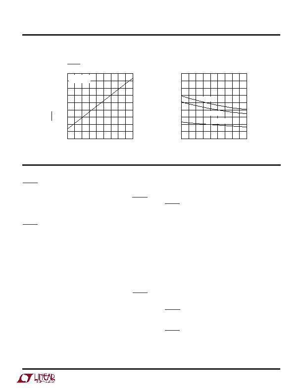
RESET Voltage vs Temperature
TEMPERATURE (癈)
55
65
0.24
0.22
0.20
0.18
0.16
0.14
0.12
0.10
0.08
0.06
1422 G19
5
35
85
25
15
105
45
125
V
CC
= 5V
3mA PULL-UP
TEMPERATURE (癈)
55
65
55
50
45
40
35
30
25
20
15
10
1422 G20
5
35
85
25
15
105
45
125
V
CC
= 12V
V
CC
= 5V
V
CC
= 3V
ON Pin Pulse (Soft Reset) Time
vs Temperature
相关PDF资料 |
PDF描述 |
|---|---|
| VE-BWZ-CX-F3 | CONVERTER MOD DC/DC 2V 30W |
| EPM570T100C3N | IC MAX II CPLD 570 LE 100-TQFP |
| MAX8860EUA25+T | IC REG LDO 2.5V/ADJ .3A 8-UMAX |
| EPM570T144C4N | IC MAX II CPLD 570 LE 144-TQFP |
| TIM396K010P0Y | CAP TANT 39UF 10V 10% RADIAL |
相关代理商/技术参数 |
参数描述 |
|---|---|
| LTC1426CMS8 | 功能描述:IC PWM D/A CONV 6BIT DUAL 8-MSOP RoHS:否 类别:集成电路 (IC) >> 数据采集 - 数模转换器 系列:- 产品培训模块:LTC263x 12-, 10-, and 8-Bit VOUT DAC Family 特色产品:LTC2636 - Octal 12-/10-/8-Bit SPI VOUT DACs with 10ppm/°C Reference 标准包装:91 系列:- 设置时间:4µs 位数:10 数据接口:MICROWIRE?,串行,SPI? 转换器数目:8 电压电源:单电源 功率耗散(最大):2.7mW 工作温度:-40°C ~ 85°C 安装类型:表面贴装 封装/外壳:14-WFDFN 裸露焊盘 供应商设备封装:14-DFN-EP(4x3) 包装:管件 输出数目和类型:8 电压,单极 采样率(每秒):* |
| LTC1426CMS8#PBF | 功能描述:IC PWM D/A CONV 6BIT DUAL 8-MSOP RoHS:是 类别:集成电路 (IC) >> 数据采集 - 数模转换器 系列:- 标准包装:2,400 系列:- 设置时间:- 位数:18 数据接口:串行 转换器数目:3 电压电源:模拟和数字 功率耗散(最大):- 工作温度:-40°C ~ 85°C 安装类型:表面贴装 封装/外壳:36-TFBGA 供应商设备封装:36-TFBGA 包装:带卷 (TR) 输出数目和类型:* 采样率(每秒):* |
| LTC1426CMS8#TR | 功能描述:IC DAC PWM 6BIT DUAL MCPWR 8MSOP RoHS:否 类别:集成电路 (IC) >> 数据采集 - 数模转换器 系列:- 产品培训模块:LTC263x 12-, 10-, and 8-Bit VOUT DAC Family 特色产品:LTC2636 - Octal 12-/10-/8-Bit SPI VOUT DACs with 10ppm/°C Reference 标准包装:91 系列:- 设置时间:4µs 位数:10 数据接口:MICROWIRE?,串行,SPI? 转换器数目:8 电压电源:单电源 功率耗散(最大):2.7mW 工作温度:-40°C ~ 85°C 安装类型:表面贴装 封装/外壳:14-WFDFN 裸露焊盘 供应商设备封装:14-DFN-EP(4x3) 包装:管件 输出数目和类型:8 电压,单极 采样率(每秒):* |
| LTC1426CMS8#TRPBF | 功能描述:IC PWM D/A CONV 6BIT DUAL 8-MSOP RoHS:是 类别:集成电路 (IC) >> 数据采集 - 数模转换器 系列:- 标准包装:2,400 系列:- 设置时间:- 位数:18 数据接口:串行 转换器数目:3 电压电源:模拟和数字 功率耗散(最大):- 工作温度:-40°C ~ 85°C 安装类型:表面贴装 封装/外壳:36-TFBGA 供应商设备封装:36-TFBGA 包装:带卷 (TR) 输出数目和类型:* 采样率(每秒):* |
| LTC1426CS8 | 功能描述:IC PWM D/A CONV 6BIT DUAL 8-SOIC RoHS:否 类别:集成电路 (IC) >> 数据采集 - 数模转换器 系列:- 产品培训模块:LTC263x 12-, 10-, and 8-Bit VOUT DAC Family 特色产品:LTC2636 - Octal 12-/10-/8-Bit SPI VOUT DACs with 10ppm/°C Reference 标准包装:91 系列:- 设置时间:4µs 位数:10 数据接口:MICROWIRE?,串行,SPI? 转换器数目:8 电压电源:单电源 功率耗散(最大):2.7mW 工作温度:-40°C ~ 85°C 安装类型:表面贴装 封装/外壳:14-WFDFN 裸露焊盘 供应商设备封装:14-DFN-EP(4x3) 包装:管件 输出数目和类型:8 电压,单极 采样率(每秒):* |
发布紧急采购,3分钟左右您将得到回复。