- 您现在的位置:买卖IC网 > PDF目录8700 > LTC1426IS8#PBF (Linear Technology)IC PWM D/A CONV 6BIT DUAL 8-SOIC PDF资料下载
参数资料
| 型号: | LTC1426IS8#PBF |
| 厂商: | Linear Technology |
| 文件页数: | 7/8页 |
| 文件大小: | 0K |
| 描述: | IC PWM D/A CONV 6BIT DUAL 8-SOIC |
| 标准包装: | 100 |
| 位数: | 6 |
| 数据接口: | 串行 |
| 转换器数目: | 2 |
| 电压电源: | 单电源 |
| 功率耗散(最大): | 550µW |
| 工作温度: | -40°C ~ 85°C |
| 安装类型: | 表面贴装 |
| 封装/外壳: | 8-SOIC(0.154",3.90mm 宽) |
| 供应商设备封装: | 8-SOIC |
| 包装: | 管件 |
| 输出数目和类型: | 2 电压,单极 |
| 采样率(每秒): | * |
7
LTC1426
TYPICAL APPLICATIONS N
U
microprocessor has “quasi-bidirectional” ports that elimi-
nate additional pull-up resistors to VCC. However, external
pull-up resistors should be used if the microprocessor
doesn’t pull the port pins high during reset.
In pulse mode, each clock pulse applied to the CLK1 or
CLK2 input increments the respective counter by one
count. When the counter increases beyond full scale
(111111B), the counter rolls over and becomes zero scale
(000000B). In this way, a single pulse applied to the CLK1
or CLK2 input increases the respective counter by one
count, and 63 pulses decrease that counter by one count.
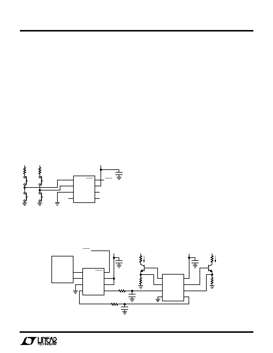
Pushbutton Mode
Figure 5 shows how to use the LTC1426 in a typical
pushbutton application. In pushbutton mode, a logic 1
pulse applied to the CLK1 or CLK2 input increments the
respective counter by one count, and stops incrementing
when the counter reaches full scale (111111B). A logic 0
pulse applied to the CLK1 or CLK2 input decrements the
respective counter by one count, and stops decrementing
when the counter reaches zero scale (000000B). An on-
chip debouncing circuit has a debounce time of 12.8ms to
prevent unintended counts with bouncing pushbuttons.
After a time delay of 410ms, the counter will begin to
increment/decrement at a repeat rate of 19.5Hz if the
pushbutton remains pressed.
Care should be taken to avoid running the CLK and PWM
traces close to one another. Since the CLK pins are high
impedance input nodes in pushbutton mode, current
spikes caused by the switching of the PWM outputs
feedthrough via any stray capacitance between PWM and
CLK lines if not properly routed. Use of proper grounding
techniques and spacing of these lines are highly recom-
mended for optimal performance.
Figure 6 shows a dual digitally programmable current
source using the LT
1013 dual precision op amp and two
NPN transistors (2N3904). After the lowpass filter combi-
nation of R1, C1 (R2, C2), its output swings from 0V to
4.93V. In the configuration shown, this voltage will be
forced across the resistor RA1(RA2). If RA1(RA2) is chosen
to be 493
, the output current will range from 0mA at zero
scale to 10mA at full scale. The minimum voltage for VS is
determined by the load resistor RL1 (RL2) and Q1(Q2)’s
VCESAT voltage. With a load resistor of 50, the voltage
source can be as low as 5V.
Information furnished by Linear Technology Corporation is believed to be accurate and reliable.
However, no responsibility is assumed for its use. Linear Technology Corporation makes no represen-
tation that the interconnection of its circuits as described herein will not infringe on existing patent rights.
Figure 6. Dual Digitally Programmable Current Source
1
2
3
4
8
7
6
5
CLK1
CLK2
GND
PWM1
SHDN
VCC
VREF
PWM2
LTC1426
PWM1
1426 F05
PWM2
PWM1/PWM2: 0V TO 0.985(VREF)
0.1
F
VREF
0V TO 5.5V
VCC
2.7V TO 5.5V
VCC
2.7V TO 5.5V
SHDN
DOWN
UP
RR
LIMITING RESISTOR R PREVENTS SHORTING OF VCC AND GND WHEN BOTH
BUTTONS ARE SIMULTANEOUSLY PUSHED. THIS RESISTOR CAN BE PLACED
EITHER IN THE VCC OR GND LEG AND THIS DETERMINES THE FUNCTION WHEN
BOTH BUTTONS ARE PUSHED. VALUE OF R < 50k
Figure 5. Pushbutton Mode Interface
1
2
3
4
8
7
6
5
CLK1
CLK2
GND
PWM1
SHDN
VCC
VREF
PWM2
P1.0
P1.1
LTC1426
1
2
3
4
8
7
6
5
OUT A
–IN A
+IN A
V –
V +
OUT B
– IN B
+ IN B
LT1013
MPU
(e.g. 8051)
0.1
F
0.1
F
RA1
493
R1
10k
5V
10V
VS
C1
0.1
F
SHDN
2N3904
R2
10k
C2
0.1
F
1426 F06
RL1
IOUT1/IOUT2: 0mA TO 10mA
RL1/RL2: <50
VS: 5V TO 30V
RL2
RA2
493
相关PDF资料 |
PDF描述 |
|---|---|
| VE-23M-IV-S | CONVERTER MOD DC/DC 10V 150W |
| VE-23H-IV-S | CONVERTER MOD DC/DC 52V 150W |
| VI-232-IV-S | CONVERTER MOD DC/DC 15V 150W |
| VI-2NM-MW-F3 | CONVERTER MOD DC/DC 10V 100W |
| VI-231-IV-S | CONVERTER MOD DC/DC 12V 150W |
相关代理商/技术参数 |
参数描述 |
|---|---|
| LTC1427CS8-50 | 功能描述:IC D/A CONV 10BIT W/SMBUS 8-SOIC RoHS:否 类别:集成电路 (IC) >> 数据采集 - 数模转换器 系列:- 产品培训模块:LTC263x 12-, 10-, and 8-Bit VOUT DAC Family 特色产品:LTC2636 - Octal 12-/10-/8-Bit SPI VOUT DACs with 10ppm/°C Reference 标准包装:91 系列:- 设置时间:4µs 位数:10 数据接口:MICROWIRE?,串行,SPI? 转换器数目:8 电压电源:单电源 功率耗散(最大):2.7mW 工作温度:-40°C ~ 85°C 安装类型:表面贴装 封装/外壳:14-WFDFN 裸露焊盘 供应商设备封装:14-DFN-EP(4x3) 包装:管件 输出数目和类型:8 电压,单极 采样率(每秒):* |
| LTC1427CS8-50#PBF | 功能描述:IC D/A CONV 10BIT W/SMBUS 8-SOIC RoHS:是 类别:集成电路 (IC) >> 数据采集 - 数模转换器 系列:- 产品培训模块:Lead (SnPb) Finish for COTS Obsolescence Mitigation Program 标准包装:50 系列:- 设置时间:4µs 位数:12 数据接口:串行 转换器数目:2 电压电源:单电源 功率耗散(最大):- 工作温度:-40°C ~ 85°C 安装类型:表面贴装 封装/外壳:8-TSSOP,8-MSOP(0.118",3.00mm 宽) 供应商设备封装:8-uMAX 包装:管件 输出数目和类型:2 电压,单极 采样率(每秒):* 产品目录页面:1398 (CN2011-ZH PDF) |
| LTC1427CS8-50#TR | 功能描述:IC DAC 10BIT SMBUS MICRPWR 8SOIC RoHS:否 类别:集成电路 (IC) >> 数据采集 - 数模转换器 系列:- 产品培训模块:LTC263x 12-, 10-, and 8-Bit VOUT DAC Family 特色产品:LTC2636 - Octal 12-/10-/8-Bit SPI VOUT DACs with 10ppm/°C Reference 标准包装:91 系列:- 设置时间:4µs 位数:10 数据接口:MICROWIRE?,串行,SPI? 转换器数目:8 电压电源:单电源 功率耗散(最大):2.7mW 工作温度:-40°C ~ 85°C 安装类型:表面贴装 封装/外壳:14-WFDFN 裸露焊盘 供应商设备封装:14-DFN-EP(4x3) 包装:管件 输出数目和类型:8 电压,单极 采样率(每秒):* |
| LTC1427CS8-50#TRPBF | 功能描述:IC D/A CONV 10BIT W/SMBUS 8-SOIC RoHS:是 类别:集成电路 (IC) >> 数据采集 - 数模转换器 系列:- 产品培训模块:LTC263x 12-, 10-, and 8-Bit VOUT DAC Family 特色产品:LTC2636 - Octal 12-/10-/8-Bit SPI VOUT DACs with 10ppm/°C Reference 标准包装:91 系列:- 设置时间:4µs 位数:10 数据接口:MICROWIRE?,串行,SPI? 转换器数目:8 电压电源:单电源 功率耗散(最大):2.7mW 工作温度:-40°C ~ 85°C 安装类型:表面贴装 封装/外壳:14-WFDFN 裸露焊盘 供应商设备封装:14-DFN-EP(4x3) 包装:管件 输出数目和类型:8 电压,单极 采样率(每秒):* |
| LTC1428CS8-50 | 功能描述:IC D/A CONV 8BIT SINK OUT 8-SOIC RoHS:否 类别:集成电路 (IC) >> 数据采集 - 数模转换器 系列:- 产品培训模块:Data Converter Fundamentals DAC Architectures 设计资源:Unipolar, Precision DC Digital-to-Analog Conversion using AD5450/1/2/3 8-14-Bit DACs (CN0052) Precision, Bipolar, Configuration for AD5450/1/2/3 8-14bit Multiplying DACs (CN0053) AC Signal Processing Using AD5450/1/2/3 Current Output DACs (CN0054) Programmable Gain Element Using AD5450/1/2/3 Current Output DAC Family (CN0055) Single Supply Low Noise LED Current Source Driver Using a Current Output DAC in the Reverse Mode (CN0139) 标准包装:10,000 系列:- 设置时间:- 位数:12 数据接口:DSP,MICROWIRE?,QSPI?,串行,SPI? 转换器数目:1 电压电源:单电源 功率耗散(最大):- 工作温度:-40°C ~ 125°C 安装类型:表面贴装 封装/外壳:SOT-23-8 薄型,TSOT-23-8 供应商设备封装:TSOT-23-8 包装:带卷 (TR) 输出数目和类型:1 电流,单极;1 电流,双极 采样率(每秒):2.7M |
发布紧急采购,3分钟左右您将得到回复。