- 您现在的位置:买卖IC网 > PDF目录149343 > LTC1430IS#PBF (LINEAR TECHNOLOGY CORP) Isolated Flyback Switching Regulator with 9V Output PDF资料下载
参数资料
| 型号: | LTC1430IS#PBF |
| 厂商: | LINEAR TECHNOLOGY CORP |
| 元件分类: | 稳压器 |
| 英文描述: | Isolated Flyback Switching Regulator with 9V Output |
| 中文描述: | SWITCHING CONTROLLER, 300 kHz SWITCHING FREQ-MAX, PDSO16 |
| 封装: | 0.150 INCH, PLASTIC, SOP-16 |
| 文件页数: | 14/16页 |
| 文件大小: | 220K |
| 代理商: | LTC1430IS#PBF |
7
LTC1430
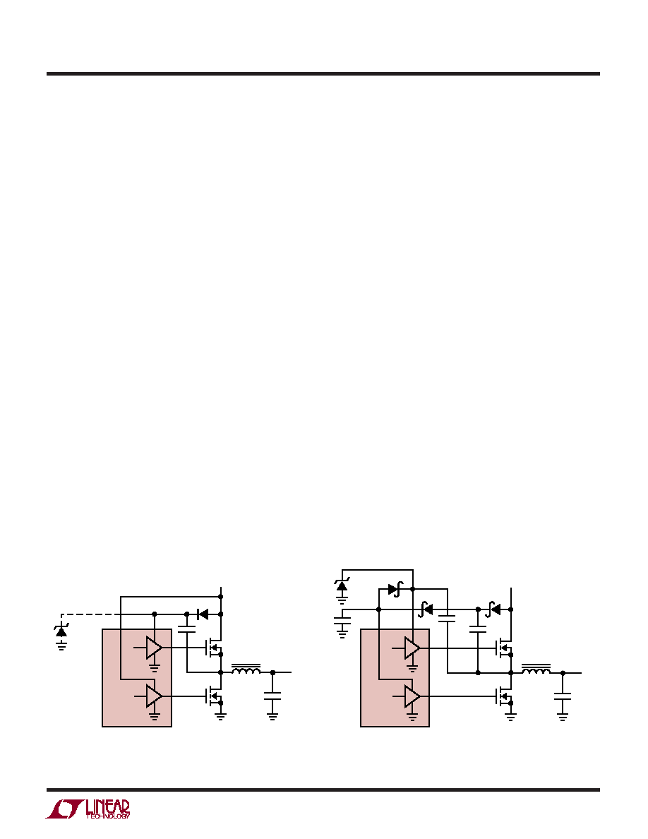
MOSFET Gate Drive
Gate drive for the top N-channel MOSFET M1 is supplied
from PVCC1. This supply must be above PVCC ( the main
power supply input) by at least one power MOSFET
VGS(ON) for efficient operation. An internal level shifter
allows PVCC1 to operate at voltages above VCC and PVCC,
up to 13V maximum. This higher voltage can be supplied
with a separate supply, or it can be generated using a
simple charge pump as shown in Figure 4. When using a
separate PVCC1 supply, the PVCC input may exhibit a large
inrush current if PVCC1 is present during power up. The
90% maximum duty cycle ensures that the charge pump
will always provide sufficient gate drive to M1. Gate drive
for the bottom MOSFET M2 is provided through PVCC2 for
16-lead devices or VCC/PVCC2 for 8-lead devices. PVCC2
can usually be driven directly from PVCC with 16-lead
parts, although it can also be charge pumped or connected
to an alternate supply if desired. The 8-lead parts require
an RC filter from PVCC to ensure proper operation; see
Input Supply Considerations.
EXTERNAL COMPONENT SELECTION
Power MOSFETs
Two N-channel power MOSFETs are required for most
LTC1430 circuits. These should be selected based prima-
rily on threshold and on-resistance considerations; ther-
mal dissipation is often a secondary concern in high
efficiency designs. Required MOSFET threshold should be
determined based on the available power supply voltages
and/or the complexity of the gate drive charge pump
scheme. In 5V input designs where an auxiliary 12V supply
is available to power PVCC1 and PVCC2, standard MOSFETs
with RDS(ON) specified at VGS = 5V or 6V can be used with
good results. The current drawn from this supply varies
with the MOSFETs used and the LTC1430’s operating
frequency, but is generally less than 50mA.
LTC1430 designs that use a doubler charge pump to
generate gate drive for M1 and run from PVCC voltages
below 7V cannot provide enough gate drive voltage to fully
enhance standard power MOSFETs. When run from 5V, a
doubler circuit may work with standard MOSFETs, but the
MOSFET RON may be quite high, raising the dissipation in
the FETs and costing efficiency. Logic level FETs are a
better choice for 5V PVCC systems; they can be fully
enhanced with a doubler charge pump and will operate at
maximum efficiency. Doubler designs running from PVCC
voltages near 4V will begin to run into efficiency problems
even with logic level FETs; such designs should be built
with tripler charge pumps (see Figure 5) or with newer,
super low threshold MOSFETs. Note that doubler charge
pump designs running from more than 7V and all tripler
charge pump designs should include a zener clamp diode
DZ at PVCC1 to prevent transients from exceeding the
absolute maximum rating at that pin.
APPLICATIO S I FOR ATIO
WU
U
Figure 4. Doubling Charge Pump
DZ
12V
1N5242
1N5817
LTC1430
PVCC1
PVCC2
0.1
F
10
F
M1
L1
M2
G1
G2
PVCC
COUT
VOUT
LTC1430 F05
+
0.1
F
1N5817
Figure 5. Tripling Charge Pump
DZ
12V
1N5242
OPTIONAL
USE FOR PVCC ≥ 7V
LTC1430
PVCC1
PVCC2
1N4148
M1
L1
M2
G1
G2
PVCC
COUT
VOUT
LTC1430 F04
+
0.1
F
相关PDF资料 |
PDF描述 |
|---|---|
| LTC1430IS#TRPBF | Isolated Flyback Switching Regulator with 9V Output |
| LTC1435AIG#TRPBF | High Efficiency Low Noise Synchronous Step-Down Switching Regulator |
| LTC1435AIS#TRPBF | High Efficiency Low Noise Synchronous Step-Down Switching Regulator |
| LTC1436ACGN#PBF | RADIATION HARDENED HIGH EFFICIENCY, 5 AMP SWITCHING REGULATORS |
| LTC1436ACGN-PLL#PBF | RADIATION HARDENED HIGH EFFICIENCY, 5 AMP SWITCHING REGULATORS |
相关代理商/技术参数 |
参数描述 |
|---|---|
| LTC1433CGN | 功能描述:IC REG BUCK 3.3V/5V/ADJ 16SSOP RoHS:否 类别:集成电路 (IC) >> PMIC - 稳压器 - DC DC 开关稳压器 系列:- 标准包装:2,500 系列:- 类型:降压(降压) 输出类型:固定 输出数:1 输出电压:1.2V,1.5V,1.8V,2.5V 输入电压:2.7 V ~ 20 V PWM 型:- 频率 - 开关:- 电流 - 输出:50mA 同步整流器:是 工作温度:-40°C ~ 125°C 安装类型:表面贴装 封装/外壳:10-TFSOP,10-MSOP(0.118",3.00mm 宽)裸露焊盘 包装:带卷 (TR) 供应商设备封装:10-MSOP 裸露焊盘 |
| LTC1433CGN#PBF | 功能描述:IC REG BUCK 3.3V/5V/ADJ 16SSOP RoHS:是 类别:集成电路 (IC) >> PMIC - 稳压器 - DC DC 开关稳压器 系列:- 标准包装:2,500 系列:- 类型:降压(降压) 输出类型:固定 输出数:1 输出电压:1.2V,1.5V,1.8V,2.5V 输入电压:2.7 V ~ 20 V PWM 型:- 频率 - 开关:- 电流 - 输出:50mA 同步整流器:是 工作温度:-40°C ~ 125°C 安装类型:表面贴装 封装/外壳:10-TFSOP,10-MSOP(0.118",3.00mm 宽)裸露焊盘 包装:带卷 (TR) 供应商设备封装:10-MSOP 裸露焊盘 |
| LTC1433CGN#TR | 功能描述:IC REG BUCK 3.3V/5V/ADJ 16SSOP RoHS:否 类别:集成电路 (IC) >> PMIC - 稳压器 - DC DC 开关稳压器 系列:- 标准包装:2,500 系列:- 类型:降压(降压) 输出类型:固定 输出数:1 输出电压:1.2V,1.5V,1.8V,2.5V 输入电压:2.7 V ~ 20 V PWM 型:- 频率 - 开关:- 电流 - 输出:50mA 同步整流器:是 工作温度:-40°C ~ 125°C 安装类型:表面贴装 封装/外壳:10-TFSOP,10-MSOP(0.118",3.00mm 宽)裸露焊盘 包装:带卷 (TR) 供应商设备封装:10-MSOP 裸露焊盘 |
| LTC1433CGN#TRPBF | 功能描述:IC REG BUCK 3.3V/5V/ADJ 16SSOP RoHS:是 类别:集成电路 (IC) >> PMIC - 稳压器 - DC DC 开关稳压器 系列:- 标准包装:20 系列:SIMPLE SWITCHER® 类型:降压(降压) 输出类型:固定 输出数:1 输出电压:12V 输入电压:4 V ~ 60 V PWM 型:电压模式 频率 - 开关:52kHz 电流 - 输出:1A 同步整流器:无 工作温度:-40°C ~ 125°C 安装类型:通孔 封装/外壳:16-DIP(0.300",7.62mm) 包装:管件 供应商设备封装:16-DIP 其它名称:*LM2575HVN-12LM2575HVN-12 |
| LTC1433IGN | 功能描述:IC REG BUCK 3.3V/5V/ADJ 16SSOP RoHS:否 类别:集成电路 (IC) >> PMIC - 稳压器 - DC DC 开关稳压器 系列:- 设计资源:Design Support Tool 标准包装:1 系列:- 类型:升压(升压) 输出类型:固定 输出数:1 输出电压:3V 输入电压:0.75 V ~ 2 V PWM 型:- 频率 - 开关:- 电流 - 输出:100mA 同步整流器:是 工作温度:-40°C ~ 85°C 安装类型:表面贴装 封装/外壳:SOT-23-5 细型,TSOT-23-5 包装:剪切带 (CT) 供应商设备封装:TSOT-23-5 其它名称:AS1323-BTTT-30CT |
发布紧急采购,3分钟左右您将得到回复。