- 您现在的位置:买卖IC网 > PDF目录1826 > LTC1430IS#PBF (Linear Technology)IC SW REG CNTRLR STEP-DWN 16SOIC PDF资料下载
参数资料
| 型号: | LTC1430IS#PBF |
| 厂商: | Linear Technology |
| 文件页数: | 7/16页 |
| 文件大小: | 0K |
| 描述: | IC SW REG CNTRLR STEP-DWN 16SOIC |
| 标准包装: | 50 |
| 应用: | 控制器,Intel Pentium? |
| 输入电压: | 4 V ~ 8 V |
| 输出数: | 1 |
| 输出电压: | 3.3V,可调 |
| 工作温度: | -40°C ~ 85°C |
| 安装类型: | 表面贴装 |
| 封装/外壳: | 16-SOIC(0.154",3.90mm 宽) |
| 供应商设备封装: | 16-SOIC |
| 包装: | 管件 |
| 产品目录页面: | 1333 (CN2011-ZH PDF) |
�� �
�
�LTC1430�
�APPLICATIO� S� I� FOR� ATIO�
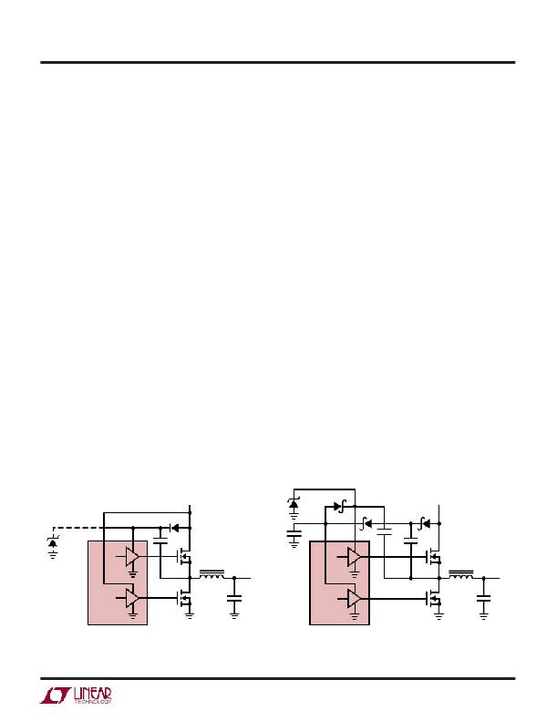
�MOSFET� Gate� Drive�
�Gate� drive� for� the� top� N-channel� MOSFET� M1� is� supplied�
�from� PV� CC1� .� This� supply� must� be� above� PV� CC� (� the� main�
�power� supply� input)� by� at� least� one� power� MOSFET�
�V� GS(ON)� for� efficient� operation.� An� internal� level� shifter�
�allows� PV� CC1� to� operate� at� voltages� above� V� CC� and� PV� CC� ,�
�up� to� 13V� maximum.� This� higher� voltage� can� be� supplied�
�with� a� separate� supply,� or� it� can� be� generated� using� a�
�simple� charge� pump� as� shown� in� Figure� 4.� When� using� a�
�separate� PV� CC1� supply,� the� PV� CC� input� may� exhibit� a� large�
�inrush� current� if� PV� CC1� is� present� during� power� up.� The�
�90%� maximum� duty� cycle� ensures� that� the� charge� pump�
�will� always� provide� sufficient� gate� drive� to� M1.� Gate� drive�
�for� the� bottom� MOSFET� M2� is� provided� through� PV� CC2� for�
�16-lead� devices� or� V� CC� /PV� CC2� for� 8-lead� devices.� PV� CC2�
�can� usually� be� driven� directly� from� PV� CC� with� 16-lead�
�parts,� although� it� can� also� be� charge� pumped� or� connected�
�to� an� alternate� supply� if� desired.� The� 8-lead� parts� require�
�an� RC� filter� from� PV� CC� to� ensure� proper� operation;� see�
�Input� Supply� Considerations.�
�EXTERNAL� COMPONENT� SELECTION�
�Power� MOSFETs�
�Two� N-channel� power� MOSFETs� are� required� for� most�
�LTC1430� circuits.� These� should� be� selected� based� prima-�
�rily� on� threshold� and� on-resistance� considerations;� ther-�
�mal� dissipation� is� often� a� secondary� concern� in� high�
�efficiency� designs.� Required� MOSFET� threshold� should� be�
�determined� based� on� the� available� power� supply� voltages�
�and/or� the� complexity� of� the� gate� drive� charge� pump�
�scheme.� In� 5V� input� designs� where� an� auxiliary� 12V� supply�
�is� available� to� power� PV� CC1� and� PV� CC2� ,� standard� MOSFETs�
�with� R� DS(ON)� specified� at� V� GS� =� 5V� or� 6V� can� be� used� with�
�good� results.� The� current� drawn� from� this� supply� varies�
�with� the� MOSFETs� used� and� the� LTC1430’s� operating�
�frequency,� but� is� generally� less� than� 50mA.�
�LTC1430� designs� that� use� a� doubler� charge� pump� to�
�generate� gate� drive� for� M1� and� run� from� PV� CC� voltages�
�below� 7V� cannot� provide� enough� gate� drive� voltage� to� fully�
�enhance� standard� power� MOSFETs.� When� run� from� 5V,� a�
�doubler� circuit� may� work� with� standard� MOSFETs,� but� the�
�MOSFET� R� ON� may� be� quite� high,� raising� the� dissipation� in�
�the� FETs� and� costing� efficiency.� Logic� level� FETs� are� a�
�better� choice� for� 5V� PV� CC� systems;� they� can� be� fully�
�enhanced� with� a� doubler� charge� pump� and� will� operate� at�
�maximum� efficiency.� Doubler� designs� running� from� PV� CC�
�voltages� near� 4V� will� begin� to� run� into� efficiency� problems�
�even� with� logic� level� FETs;� such� designs� should� be� built�
�with� tripler� charge� pumps� (see� Figure� 5)� or� with� newer,�
�super� low� threshold� MOSFETs.� Note� that� doubler� charge�
�pump� designs� running� from� more� than� 7V� and� all� tripler�
�charge� pump� designs� should� include� a� zener� clamp� diode�
�D� Z� at� PV� CC1� to� prevent� transients� from� exceeding� the�
�absolute� maximum� rating� at� that� pin.�
�PV� CC�
�D� Z�
�12V�
�1N5817�
�PV� CC�
�OPTIONAL�
�USE� FOR� PV� CC� ≥� 7V�
�1N4148�
�1N5242�
�1N5817�
�1N5817�
�D� Z�
�12V�
�PV� CC2�
�PV� CC1�
�0.1� μ� F�
�10� μ� F�
�PV� CC2�
�PV� CC1�
�0.1� μ� F�
�0.1� μ� F�
�1N5242�
�G1�
�M1�
�G1�
�M1�
�L1�
�V� OUT�
�L1�
�V� OUT�
�G2�
�M2�
�+�
�C� OUT�
�G2�
�M2�
�+�
�C� OUT�
�LTC1430�
�Figure� 4.� Doubling� Charge� Pump�
�LTC1430� ?� F04�
�LTC1430�
�Figure� 5.� Tripling� Charge� Pump�
�LTC1430� ?� F05�
�7�
�相关PDF资料 |
PDF描述 |
|---|---|
| LTC1434CGN#PBF | IC REG BUCK 3.3V/5V/ADJ 20SSOP |
| LTC1435CG#PBF | IC REG CTRLR BUCK PWM CM 16-SSOP |
| LTC1436AEGN#TRPBF | IC REG CTRLR BUCK PWM CM 24-SSOP |
| LTC1439EG#TRPBF | IC REG CTRLR BUCK PWM CM 36-SSOP |
| LTC1473IGN#TRPBF | IC SWITCH DVR PWRPATH DUAL16SSOP |
相关代理商/技术参数 |
参数描述 |
|---|---|
| LTC1433CGN | 功能描述:IC REG BUCK 3.3V/5V/ADJ 16SSOP RoHS:否 类别:集成电路 (IC) >> PMIC - 稳压器 - DC DC 开关稳压器 系列:- 标准包装:2,500 系列:- 类型:降压(降压) 输出类型:固定 输出数:1 输出电压:1.2V,1.5V,1.8V,2.5V 输入电压:2.7 V ~ 20 V PWM 型:- 频率 - 开关:- 电流 - 输出:50mA 同步整流器:是 工作温度:-40°C ~ 125°C 安装类型:表面贴装 封装/外壳:10-TFSOP,10-MSOP(0.118",3.00mm 宽)裸露焊盘 包装:带卷 (TR) 供应商设备封装:10-MSOP 裸露焊盘 |
| LTC1433CGN#PBF | 功能描述:IC REG BUCK 3.3V/5V/ADJ 16SSOP RoHS:是 类别:集成电路 (IC) >> PMIC - 稳压器 - DC DC 开关稳压器 系列:- 标准包装:2,500 系列:- 类型:降压(降压) 输出类型:固定 输出数:1 输出电压:1.2V,1.5V,1.8V,2.5V 输入电压:2.7 V ~ 20 V PWM 型:- 频率 - 开关:- 电流 - 输出:50mA 同步整流器:是 工作温度:-40°C ~ 125°C 安装类型:表面贴装 封装/外壳:10-TFSOP,10-MSOP(0.118",3.00mm 宽)裸露焊盘 包装:带卷 (TR) 供应商设备封装:10-MSOP 裸露焊盘 |
| LTC1433CGN#TR | 功能描述:IC REG BUCK 3.3V/5V/ADJ 16SSOP RoHS:否 类别:集成电路 (IC) >> PMIC - 稳压器 - DC DC 开关稳压器 系列:- 标准包装:2,500 系列:- 类型:降压(降压) 输出类型:固定 输出数:1 输出电压:1.2V,1.5V,1.8V,2.5V 输入电压:2.7 V ~ 20 V PWM 型:- 频率 - 开关:- 电流 - 输出:50mA 同步整流器:是 工作温度:-40°C ~ 125°C 安装类型:表面贴装 封装/外壳:10-TFSOP,10-MSOP(0.118",3.00mm 宽)裸露焊盘 包装:带卷 (TR) 供应商设备封装:10-MSOP 裸露焊盘 |
| LTC1433CGN#TRPBF | 功能描述:IC REG BUCK 3.3V/5V/ADJ 16SSOP RoHS:是 类别:集成电路 (IC) >> PMIC - 稳压器 - DC DC 开关稳压器 系列:- 标准包装:20 系列:SIMPLE SWITCHER® 类型:降压(降压) 输出类型:固定 输出数:1 输出电压:12V 输入电压:4 V ~ 60 V PWM 型:电压模式 频率 - 开关:52kHz 电流 - 输出:1A 同步整流器:无 工作温度:-40°C ~ 125°C 安装类型:通孔 封装/外壳:16-DIP(0.300",7.62mm) 包装:管件 供应商设备封装:16-DIP 其它名称:*LM2575HVN-12LM2575HVN-12 |
| LTC1433IGN | 功能描述:IC REG BUCK 3.3V/5V/ADJ 16SSOP RoHS:否 类别:集成电路 (IC) >> PMIC - 稳压器 - DC DC 开关稳压器 系列:- 设计资源:Design Support Tool 标准包装:1 系列:- 类型:升压(升压) 输出类型:固定 输出数:1 输出电压:3V 输入电压:0.75 V ~ 2 V PWM 型:- 频率 - 开关:- 电流 - 输出:100mA 同步整流器:是 工作温度:-40°C ~ 85°C 安装类型:表面贴装 封装/外壳:SOT-23-5 细型,TSOT-23-5 包装:剪切带 (CT) 供应商设备封装:TSOT-23-5 其它名称:AS1323-BTTT-30CT |
发布紧急采购,3分钟左右您将得到回复。