- 您现在的位置:买卖IC网 > PDF目录8981 > LTC1454LCS#PBF (Linear Technology)IC D/A CONV 12BIT R-R DUAL16SOIC PDF资料下载
参数资料
| 型号: | LTC1454LCS#PBF |
| 厂商: | Linear Technology |
| 文件页数: | 10/12页 |
| 文件大小: | 0K |
| 描述: | IC D/A CONV 12BIT R-R DUAL16SOIC |
| 标准包装: | 50 |
| 设置时间: | 14µs |
| 位数: | 12 |
| 数据接口: | 串行 |
| 转换器数目: | 2 |
| 电压电源: | 单电源 |
| 功率耗散(最大): | 1.35mW |
| 工作温度: | 0°C ~ 70°C |
| 安装类型: | 表面贴装 |
| 封装/外壳: | 16-SOIC(0.154",3.90mm 宽) |
| 供应商设备封装: | 16-SOIC |
| 包装: | 管件 |
| 输出数目和类型: | 2 电压,单极 |
| 采样率(每秒): | * |
| 产品目录页面: | 1350 (CN2011-ZH PDF) |
7
LTC1454/LTC1454L
DEFI ITIO S
UU
LSB = (VFS – VOS)/(2n – 1) = (VFS – VOS)/4095
Nominal LSBs:
LTC1454
LSB = 4.095V/4095 = 1mV
LTC1454L
LSB = 2.5V/4095 = 0.610mV
Integral Nonlinearity (INL): End-point INL is the maxi-
mum deviation from a straight line passing through the
end-points of the DAC transfer curve. Because the part
operates from a single supply and the output cannot go
below zero, the linearity is measured between full scale
and the code corresponding to the maximum offset speci-
fication. The INL error at a given input code is calculated
as follows:
INL
= [VOUT – VOS – (VFS – VOS)(Code/4095)]/LSB
VOUT = The output voltage of the DAC measured at
the given input code
Differential Nonlinearity (DNL): DNL is the difference
between the measured change and the ideal 1LSB change
between any two adjacent codes. The DNL error between
any two codes is calculated as follows:
DNL
= (
VOUT – LSB)/LSB
VOUT = The measured voltage difference between
two adjacent codes
Digital Feedthrough: The glitch that appears at the analog
output caused by AC coupling from the digital inputs when
they change state. The area of the glitch is specified in
(nV)(sec).
Resolution (n): Resolution is defined as the number of
digital input bits, n. It defines the number of DAC output
states (2n) that divide the full-scale range. The resolution
does not imply linearity.
Full-Scale Voltage (VFS): This is the output of the DAC
when all bits are set to 1.
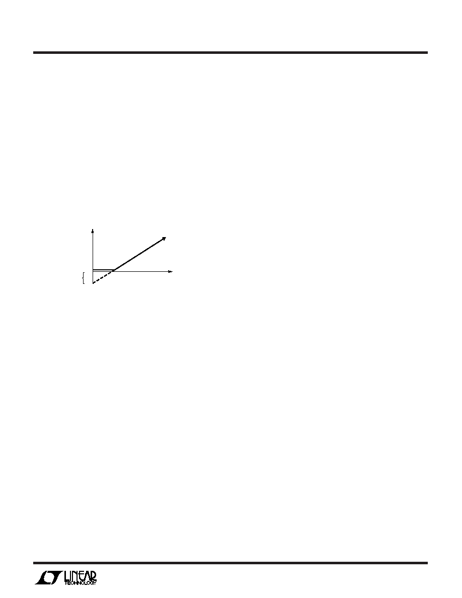
Voltage Offset Error (VOS): The theoretical voltage at the
output when the DAC is loaded with all zeros. The output
amplifier can have a true negative offset, but because the
part is operated from a single supply, the output cannot go
below zero. If the offset is negative, the output will remain
near 0V resulting in the transfer curve shown in Figure 1.
DAC CODE
LTC1454/5 F01
OUTPUT
VOLTAGE
NEGATIVE
OFFSET
0V
Figure 1. Effect of Negative Offset
The offset of the part is measured at the code that corre-
sponds to the maximum offset specification:
VOS = VOUT – (Code)(VFS)/(2n – 1)
Least Significant Bit (LSB): One LSB is the ideal voltage
difference between two successive codes.
相关PDF资料 |
PDF描述 |
|---|---|
| VE-J0R-MZ-F4 | CONVERTER MOD DC/DC 7.5V 25W |
| GTC00CF-24-28S | CONN RCPT 24POS WALL MNT W/SCKT |
| M83723/96W1808N | CONN PLUG 8POS STRAIGHT W/PINS |
| GTC06CF-28-16S | CONN PLUG 20POS STRAIGHT W/SCKT |
| 206613-3 | CONN RECEPT CPC 22POS STD SER 4 |
相关代理商/技术参数 |
参数描述 |
|---|---|
| LTC1454LIN | 功能描述:IC DAC 12BIT R-R DUAL 3V 16DIP RoHS:否 类别:集成电路 (IC) >> 数据采集 - 数模转换器 系列:- 标准包装:47 系列:- 设置时间:2µs 位数:14 数据接口:并联 转换器数目:1 电压电源:单电源 功率耗散(最大):55µW 工作温度:-40°C ~ 85°C 安装类型:表面贴装 封装/外壳:28-SSOP(0.209",5.30mm 宽) 供应商设备封装:28-SSOP 包装:管件 输出数目和类型:1 电流,单极;1 电流,双极 采样率(每秒):* |
| LTC1454LIN#PBF | 功能描述:IC D/A CONV 12BIT R-R DUAL 16DIP RoHS:是 类别:集成电路 (IC) >> 数据采集 - 数模转换器 系列:- 标准包装:2,400 系列:- 设置时间:- 位数:18 数据接口:串行 转换器数目:3 电压电源:模拟和数字 功率耗散(最大):- 工作温度:-40°C ~ 85°C 安装类型:表面贴装 封装/外壳:36-TFBGA 供应商设备封装:36-TFBGA 包装:带卷 (TR) 输出数目和类型:* 采样率(每秒):* |
| LTC1454LIS | 功能描述:IC D/A CONV 12BIT R-R DUAL16SOIC RoHS:否 类别:集成电路 (IC) >> 数据采集 - 数模转换器 系列:- 标准包装:47 系列:- 设置时间:2µs 位数:14 数据接口:并联 转换器数目:1 电压电源:单电源 功率耗散(最大):55µW 工作温度:-40°C ~ 85°C 安装类型:表面贴装 封装/外壳:28-SSOP(0.209",5.30mm 宽) 供应商设备封装:28-SSOP 包装:管件 输出数目和类型:1 电流,单极;1 电流,双极 采样率(每秒):* |
| LTC1454LIS#PBF | 功能描述:IC D/A CONV 12BIT R-R DUAL16SOIC RoHS:是 类别:集成电路 (IC) >> 数据采集 - 数模转换器 系列:- 标准包装:47 系列:- 设置时间:2µs 位数:14 数据接口:并联 转换器数目:1 电压电源:单电源 功率耗散(最大):55µW 工作温度:-40°C ~ 85°C 安装类型:表面贴装 封装/外壳:28-SSOP(0.209",5.30mm 宽) 供应商设备封装:28-SSOP 包装:管件 输出数目和类型:1 电流,单极;1 电流,双极 采样率(每秒):* |
| LTC1454LIS#TR | 功能描述:IC DAC 12BIT R-R DUAL 3V 16SOIC RoHS:否 类别:集成电路 (IC) >> 数据采集 - 数模转换器 系列:- 标准包装:47 系列:- 设置时间:2µs 位数:14 数据接口:并联 转换器数目:1 电压电源:单电源 功率耗散(最大):55µW 工作温度:-40°C ~ 85°C 安装类型:表面贴装 封装/外壳:28-SSOP(0.209",5.30mm 宽) 供应商设备封装:28-SSOP 包装:管件 输出数目和类型:1 电流,单极;1 电流,双极 采样率(每秒):* |
发布紧急采购,3分钟左右您将得到回复。