- 您现在的位置:买卖IC网 > PDF目录10191 > LTC1483CN8 (Linear Technology)IC TXRX RS485 LOW EMI LOPWR 8DIP PDF资料下载
参数资料
| 型号: | LTC1483CN8 |
| 厂商: | Linear Technology |
| 文件页数: | 6/8页 |
| 文件大小: | 0K |
| 描述: | IC TXRX RS485 LOW EMI LOPWR 8DIP |
| 标准包装: | 50 |
| 类型: | 收发器 |
| 驱动器/接收器数: | 1/1 |
| 规程: | RS422,RS485 |
| 电源电压: | 4.75 V ~ 5.25 V |
| 安装类型: | 通孔 |
| 封装/外壳: | 8-DIP(0.300",7.62mm) |
| 供应商设备封装: | 8-PDIP |
| 包装: | 管件 |
6
LTC1483
sn1483 1483fs
SWITCHI G TI E WAVEFOR S
UW
W
1.5V
tPHL
RO
–VOD2
A – B
0V
1.5V
tPLH
OUTPUT
INPUT
VOD2
VOL
VOH
LTC1483 F07
tr ≤ 10ns, tf ≤ 10ns
Figure 7. Receiver Propagation Delays
1.5V
tZL(SHDN), tZL
tZH(SHDN), tZH
1.5V
tLZ
0.5V
tHZ
OUTPUT NORMALLY LOW
OUTPUT NORMALLY HIGH
3V
0V
RE
5V
0V
RO
LTC1483 F08
tr ≤ 10ns, tf ≤ 10ns
Figure 8. Receiver Enable and Disable Times
APPLICATIO S I FOR ATIO
UU
W
U
Basic Theory of Operation
Traditionally RS485 transceivers have been designed us-
ing bipolar technology because the common-mode range
of the device must extend beyond the supplies and the
device must be immune to ESD damage and latch-up.
Unfortunately, most bipolar devices draw a large amount
of supply current, which is unacceptable for the numerous
applications that require low power consumption. The
LTC1483 is a CMOS RS485/RS422 transceiver which
features ultra-low power consumption without sacrificing
ESD and latch-up immunity.
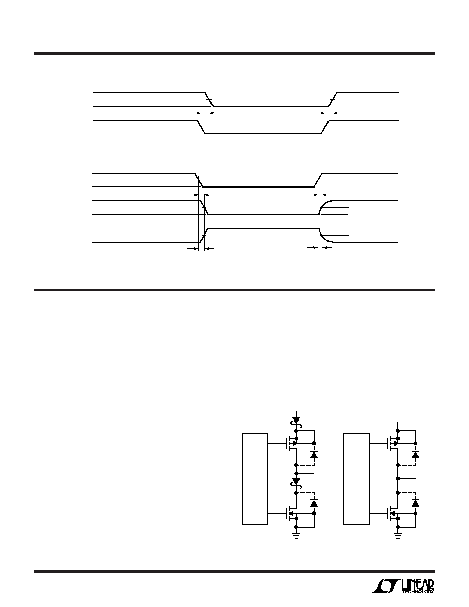
The LTC1483 uses a proprietary driver output stage,
which allows a common-mode range that extends beyond
the power supplies while virtually eliminating latch-up and
providing excellent ESD protection. Figure 9 shows the
LTC1483 output stage while Figure 10 shows a conven-
tional CMOS output stage.
When the conventional CMOS output stage of Figure 10
enters a high impedance state, both the P-channel (P1)
and the N-channel (N1) are turned off. If the output is then
driven above VCC or below ground, the P+/N -well diode
(D1) or the N+/P-substrate diode (D2) respectively will
turn on and clamp the output to the supply. Thus, the
output stage is no longer in a high impedance state and is
not able to meet the RS485 common-mode range require-
ment. In addition, the large amount of current flowing
through either diode will induce the well-known CMOS
latch-up condition, which could destroy the device.
LOGIC
VCC
SD3
P1
D1
OUTPUT
SD4
D2
N1
LTC1483 F09
Figure 9. LTC1483 Output Stage
LOGIC
VCC
P1
D1
OUTPUT
D2
N1
LTC1483 F10
Figure 10. Conventional
CMOS Output Stage
相关PDF资料 |
PDF描述 |
|---|---|
| LTC1487CN8#PBF | IC TXRX RS485 LOW EMI LOPWR 8DIP |
| VE-B20-MY | CONVERTER MOD DC/DC 5V 50W |
| CXC3102A2428P | CONN RCPT 24POS PNL MNT PIN |
| MS27484E12A3S | CONN PLUG 3POS STRAIGHT W/SCKT |
| VE-JW4-MX-S | CONVERTER MOD DC/DC 48V 75W |
相关代理商/技术参数 |
参数描述 |
|---|---|
| LTC1483CN8#PBF | 功能描述:IC TXRX RS485 LOW EMI LOPWR 8DIP RoHS:是 类别:集成电路 (IC) >> 接口 - 驱动器,接收器,收发器 系列:- 产品培训模块:RS-232 & USB Transceiver 标准包装:2,000 系列:- 类型:收发器 驱动器/接收器数:1/1 规程:RS232 电源电压:3 V ~ 5.5 V 安装类型:表面贴装 封装/外壳:16-SSOP(0.209",5.30mm 宽) 供应商设备封装:16-SSOP 包装:带卷 (TR) 其它名称:296-19849-2 |
| LTC1483CN8PBF | 制造商:Linear Technology 功能描述:RS-485 Driver/Receiver 120uA LowEMI DIP8 |
| LTC1483CS8 | 功能描述:IC TXRX RS485 LOW EMI LOPWR8SOIC RoHS:否 类别:集成电路 (IC) >> 接口 - 驱动器,接收器,收发器 系列:- 标准包装:121 系列:- 类型:收发器 驱动器/接收器数:1/1 规程:RS422,RS485 电源电压:3 V ~ 3.6 V 安装类型:表面贴装 封装/外壳:10-WFDFN 裸露焊盘 供应商设备封装:10-DFN(3x3) 包装:管件 |
| LTC1483CS8#PBF | 功能描述:IC TXRX RS485 LOW EMI LOPWR8SOIC RoHS:是 类别:集成电路 (IC) >> 接口 - 驱动器,接收器,收发器 系列:- 产品培训模块:RS-232 & USB Transceiver 标准包装:2,000 系列:- 类型:收发器 驱动器/接收器数:1/1 规程:RS232 电源电压:3 V ~ 5.5 V 安装类型:表面贴装 封装/外壳:16-SSOP(0.209",5.30mm 宽) 供应商设备封装:16-SSOP 包装:带卷 (TR) 其它名称:296-19849-2 |
| LTC1483CS8#TR | 功能描述:IC TXRX RS485 LO EMI SHTDN 8SOIC RoHS:否 类别:集成电路 (IC) >> 接口 - 驱动器,接收器,收发器 系列:- 标准包装:121 系列:- 类型:收发器 驱动器/接收器数:1/1 规程:RS422,RS485 电源电压:3 V ~ 3.6 V 安装类型:表面贴装 封装/外壳:10-WFDFN 裸露焊盘 供应商设备封装:10-DFN(3x3) 包装:管件 |
发布紧急采购,3分钟左右您将得到回复。