- 您现在的位置:买卖IC网 > PDF目录383291 > LTC1531CSW (LINEAR TECHNOLOGY CORP) Self-Powered Isolated Comparator PDF资料下载
参数资料
| 型号: | LTC1531CSW |
| 厂商: | LINEAR TECHNOLOGY CORP |
| 元件分类: | 运动控制电子 |
| 英文描述: | Self-Powered Isolated Comparator |
| 中文描述: | COMPARATOR, PDSO28 |
| 封装: | 0.300 INCH, PLASTIC, SOP-28 |
| 文件页数: | 7/16页 |
| 文件大小: | 266K |
| 代理商: | LTC1531CSW |
7
LTC1531
APPLICATIO
S I
N
FOR
ATIO
U
W
U
tance, which will subsequently be discharged between
samples, will consume power from V
PW
.
ISOLATED COMPARATOR INPUTS AND CMPOUT
The LTC1531 isolated comparator has a 4-input
summing comparator that performs the following
comparison:
(V1 + V2)/2 > (V3 + V4)/2
By rearranging the equation, for example, a dual differen-
tial comparison is performed:
(V1 – V4) > (V3 – V2) or (V1 – V3) > (V4 – V2)
The input has a rail-to-rail input and common mode
voltage range of V
PW
-ISOGND. The summing nature of the
inputs allows midsupply referencing. For example, con-
necting V3 to V
REG
and V4 to ISOGND sums together to
provide V
REG
/2 for the negative comparator input. See for
example, the Isolated Switch Control.
Charge injection and leakage currents occur at the com-
parator inputs. The amount depends on how the compara-
tor is used. Minimum leakage currents occur with V1 = V2
and V3 = V4 where the input impedance is from charge
injection and is nominally 300M
. When V1
≠
V2 or
V3
≠
V4, the input impedance due to leakage currents is
about 15M
to 20M
. Since the comparator is turned on
only for the last 10
μ
s of the 108
μ
s V
REG
period, the charge
injection occurs at about the 98
μ
s point with a coupling
capacitance of 2pF per input.
The CMPOUT signal is typically used to provide hyster-
esis, as in the Isolated Temperature Control application.
CMPOUT is the latched result of the previous comparison
and is active during the following V
REG
ON period. CMPOUT
is powered by V
REG
, the internal 2.5V regulated output,
and is in high impedance except during the 108
μ
s
V
REG
ON time. When active, CMPOUT is switched low to
ISOGND or high to V
REG
depending on the stored result of
the previous comparison. The stored CMPOUT data is
reset during power-up. CMPOUT is not necessarily reset
by the powered side SHDN pin, except when shutdown
results in V
PW
drooping low enough to trigger a power-on
reset on the isolated side between 1.5V to 2.5V.
DATA, VALID, ZCDATA
During a power cycle, the VALID signal goes high if a valid
comparison was made during the previous listen cycle.
VALID goes low at the beginning of the next listen cycle.
The low-to-high transition of VALID can be used to clock
DATA into external circuitry. VALID is delayed 200ns after
the DATA output. In order for a comparison to occur,
sufficient power must be stored on the isolated side
storage capacitor.
The DATA output holds the last received compare result.
DATA is reset to zero on power-up and shutdown. The
VALID output is held high for one power cycle following a
correctly received compare result. The received DATA
value from the isolated side contains redundancy to im-
prove noise immunity.
The ZCDATA is a 25
μ
s output pulse triggered by the zero-
cross comparator. In order for a pulse to occur, the DATA
output must be at logic 1 and the ZCPOS-ZCNEG zero-
cross comparator input crosses 0V after the input has
exceeded the
±
150mV to 800mV of hysteresis. The zero-
cross comparator output is typically used to trigger a triac
from a 60Hz RC phase shifted AC line signal. See Typical
Applications.
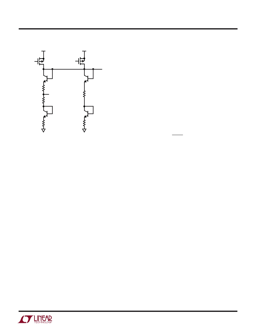
Figure 5. V
REG
Output Stage
V
PW
V
REG
1531 F05
23k
16k
ISOGND
V
PW
V
GP
21k
2k
16k
1
ISOGND
1
相关PDF资料 |
PDF描述 |
|---|---|
| LTC1531 | Self-Powered Isolated Comparator |
| LTC1535CSW | Isolated RS485 Transceiver |
| LTC1535 | Isolated RS485 Transceiver |
| LTC1540IS8 | Nanopower Comparator with Reference |
| LTC1540 | Nanopower Comparator with Reference |
相关代理商/技术参数 |
参数描述 |
|---|---|
| LTC1531CSW#PBF | 功能描述:IC COMP ISOLATED SLF-PWRD 28SOIC RoHS:是 类别:集成电路 (IC) >> 线性 - 比较器 系列:- 产品培训模块:Lead (SnPb) Finish for COTS Obsolescence Mitigation Program 标准包装:2,500 系列:- 类型:通用 元件数:1 输出类型:CMOS,推挽式,满摆幅,TTL 电压 - 电源,单路/双路(±):2.5 V ~ 5.5 V,±1.25 V ~ 2.75 V 电压 - 输入偏移(最小值):5mV @ 5.5V 电流 - 输入偏压(最小值):1pA @ 5.5V 电流 - 输出(标准):- 电流 - 静态(最大值):24µA CMRR, PSRR(标准):80dB CMRR,80dB PSRR 传输延迟(最大):450ns 磁滞:±3mV 工作温度:-40°C ~ 85°C 封装/外壳:6-WFBGA,CSPBGA 安装类型:表面贴装 包装:管件 其它名称:Q3554586 |
| LTC1531CSW#TR | 功能描述:IC COMP DIFF DUAL SELFPWR 28SOIC RoHS:否 类别:集成电路 (IC) >> 线性 - 比较器 系列:- 产品培训模块:Lead (SnPb) Finish for COTS Obsolescence Mitigation Program 标准包装:2,500 系列:- 类型:通用 元件数:1 输出类型:CMOS,推挽式,满摆幅,TTL 电压 - 电源,单路/双路(±):2.5 V ~ 5.5 V,±1.25 V ~ 2.75 V 电压 - 输入偏移(最小值):5mV @ 5.5V 电流 - 输入偏压(最小值):1pA @ 5.5V 电流 - 输出(标准):- 电流 - 静态(最大值):24µA CMRR, PSRR(标准):80dB CMRR,80dB PSRR 传输延迟(最大):450ns 磁滞:±3mV 工作温度:-40°C ~ 85°C 封装/外壳:6-WFBGA,CSPBGA 安装类型:表面贴装 包装:管件 其它名称:Q3554586 |
| LTC1531CSW#TRPBF | 功能描述:IC COMP ISOLATED SLF-PWRD 28SOIC RoHS:是 类别:集成电路 (IC) >> 线性 - 比较器 系列:- 产品培训模块:Lead (SnPb) Finish for COTS Obsolescence Mitigation Program 标准包装:2,500 系列:- 类型:通用 元件数:1 输出类型:CMOS,推挽式,满摆幅,TTL 电压 - 电源,单路/双路(±):2.5 V ~ 5.5 V,±1.25 V ~ 2.75 V 电压 - 输入偏移(最小值):5mV @ 5.5V 电流 - 输入偏压(最小值):1pA @ 5.5V 电流 - 输出(标准):- 电流 - 静态(最大值):24µA CMRR, PSRR(标准):80dB CMRR,80dB PSRR 传输延迟(最大):450ns 磁滞:±3mV 工作温度:-40°C ~ 85°C 封装/外壳:6-WFBGA,CSPBGA 安装类型:表面贴装 包装:管件 其它名称:Q3554586 |
| LTC1531IS8 | 制造商:Linear Technology 功能描述:Self-Powered Isolated Comparator |
| LTC1535CSW | 功能描述:IC LINE TRANSCEIVER 28-SOIC RoHS:否 类别:集成电路 (IC) >> 接口 - 驱动器,接收器,收发器 系列:- 标准包装:27 系列:- 类型:收发器 驱动器/接收器数:3/3 规程:RS232,RS485 电源电压:4.75 V ~ 5.25 V 安装类型:表面贴装 封装/外壳:28-SOIC(0.295",7.50mm 宽) 供应商设备封装:28-SOIC 包装:管件 |
发布紧急采购,3分钟左右您将得到回复。